Power supply device for out putting stable programmable power supply

Inactive Publication Date: 2005-11-17
GRAND POWER SOURCES
6 Cites 4 Cited by

AI-Extracted Technical Summary

Problems solved by technology

Although the linear power supply device is popular, yet it still has certain shortcomings including a large power loss and a low power efficiency.
Further, since the volume of the power supply device used for the instrument is large and inefficient, therefore it is a trend of using a switching-mode technique for the manufacture of the power supply device for instruments, and such technology is used to provide a power density and a power efficiency.
However, the traditional linear power supply device generally uses a transistor working in a linear area and using it as a rheostat to modulate unstable input voltages.
Therefore, the total system power loss will be increased, and the efficiency will drop.
However, the switching power supply does not work ...

Benefits of technology

[0012] A further objective of the present invention is to provide a power supply device for outputting a stable power supply, which comprises a voltage divider circuit connected to a DC power supply of a rectify/filter circuit disposed at the input terminal of the power supply device, and the voltage divider circuit is also connected to an input terminal of an IC of the pulse width modulator, so that if a voltage OVRV exceeds a predetermined value due to an excessively high AC power supply, the OVRV will turn off the MOSFET to protect the power supply device and avoid damages caused by the high voltage. In the same time, the present invention will also provide a bias voltage circuit for the primary driver circuit of the transfor...

Abstract

The present invention discloses a power supply device for outputting a stable programmable power supply, which comprises a transformer disposed at a DC output end of the power supply device, and a clamp circuit connected to a secondary current of the transformer. Since the clamp circuit is disposed on the secondary current of the transformer, therefore it does not require a high DC voltage to drive the clamp circuit. The clamp circuit can release the high voltage produced when the metal oxide semiconductor field effect transistor (MOSFET) is off, and thus reducing the high voltage borne by the MOSFET to enhance the reliability of the MOSFET. Additionally, the present invention can prevent the transformer from being saturated due to magnetic leakage, inductance, and stored energies released or eliminated from the transformer.

Application Domain

Emergency protective circuit arrangementsApparatus with intermediate ac conversion +2

Technology Topic

Oxide semiconductorMOSFET +8

Image

  • Power supply device for out putting stable programmable power supply
  • Power supply device for out putting stable programmable power supply
  • Power supply device for out putting stable programmable power supply

Examples

  • Experimental program(1)

Example

[0019] To make it easier for our examiner to understand the objective of the invention, its structure, innovative features, and performance, we use a preferred embodiment together with the attached drawings for the detailed description of the invention.
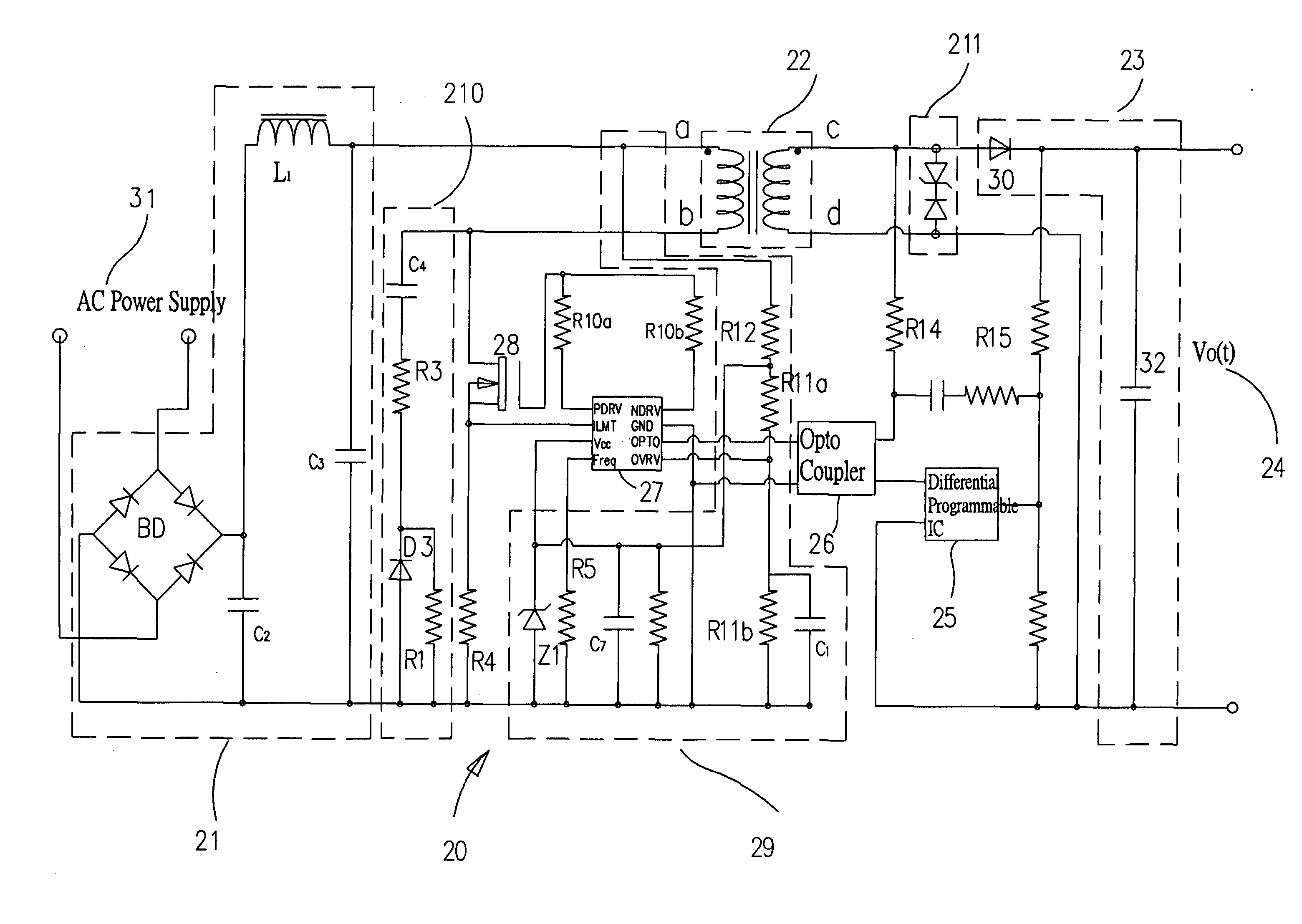
[0020] The present invention discloses a power supply device for outputting a stable programmable power supply. Please refer to FIGS. 2 and 3. The power supply device 20 comprises a rectify/filter circuit 21, a transformer 22, a secondary filter circuit 23, and a DC output terminal 24; wherein the rectify/filter circuit 21 is connected to an AC power supply 31, and a capacitor C2 and an inductor L1 constitute a full wave rectify circuit for rectifying and filtering the AC power supply 31 to obtain a more stable DC power supply, and the transformer 22 is connected to a rectify/filter circuit 21 for rectifying and filtering and lowering the voltage of the AC power supply modulated by the programmable switching circuit. After a secondary filter made by a secondary filter circuit, the DC power supply is outputted from the DC output terminal 24.
[0021] Further, please refer to FIGS. 4 and 5. A differential programmable IC 25 is disposed between the DC terminal 24 of the power supply device 20 and the secondary filter circuit 23, so that the comparison function of a differential programmable IC 25 is used to compare the output voltage of the DC output terminal with a predetermined voltage/time programmable control, and the difference after the comparison is sent to a pulse width modulation IC (PWM IC) 27. The PWM IC 27 controls the waveform loading cycle of a metal oxide semiconductor field effect transistor (MOSFET) 28 disposed between the rectify/filter circuit 21 and the transformer 22 according to such difference, and modulates the ratio of ON-OFF current of the primary input power of the transformer 22 and further provide a constant voltage output from the DC output terminal 24 of the power supply device 20.
[0022] Please refer to FIG. 4 and 5 again. In the invention, the power supply device 20 comprises a voltage divider circuit 29, and the voltage divider circuit 29 is connected to a rectify/filter circuit 21 at the output terminal of the power supply device 20. The voltage divider circuit 29 is connected to an OVRV terminal of a pulse width modulation IC 27, and the voltage divider circuit 29 sends the DC voltage of the rectify/filter circuit 21 to the PWM IC 27, such that when the OVRV voltage occurs due to an excessively high voltage and the rectified DC voltage exceeds a predetermined value, the OVRV turns off the MOSFET 29 to protect the power supply device 20 from being damaged by the high voltage.
[0023] Please refer to FIGS. 4 and 5 again. In the invention, the power supply device 20 comprises a buffer circuit 210 comprised of a capacitor C4, a resistor R3, R1, and a diode D3. The buffer circuit 210 is connected to the MOSFET 28, and can prevent a surge and a high voltage caused by the reverse direction of the voltage when the transformer 22 turns off the MOSFET 28. When the MOSFET 28 is turned off, the diode D3 is in reverse bias voltage to charge a high voltage pulse produced by the One Aspect Circuit 26b of the transformer 22 by a capacitor C4 to absorb such purge. When the MOSFET 28 is turned on, the diode D3 is in the forward bias voltage and discharges the capacitor C4 to consume the power of the surge and protect the MOSFET 28 and reduce the generation of electromagnetic interference signals.
[0024] Please refer to FIGS. 4 and 5 again. In the invention, the power supply device 20 comprises a clamp circuit 211. With the connection to a magnetic circuit of the transformer 22, the clamp circuit 211 is connected to the Another Aspect Circuit of the transformer, so that the clamp circuit 211 can release the high voltage produced when the MOSFET 28 is turned off and the energy produced by a magnetic leakage and an inductance of the transformer 22 and then stored in the transformer 22, and thus lowering the high voltage borne by the MOSFET 28 and enhancing the reliability of the MOSFET 28.
[0025] Please refer to FIGS. 4 and 5. In the invention, the clamp circuit 211 releases energy by converting the reverse bias voltage of a diode into a forward bias voltage when the MOSFET 28 is turned off. The Zener diode is in reverse bias voltage, such that the Zener diode can discharge itself to release and eliminate the energy when the power exceeds a normal rated reference reverse voltage, and also can prevent the saturation of the transformer 22.
[0026] Please refer to FIGS. 4 and 5. In the invention, the primary terminal a of the transformer 22 is connected to the positive terminal at the rear of the rectify/filter circuit 21, and the rectified negative terminal is connected to the common ground terminal.
[0027] Please refer to FIGS. 4 and 5. In the invention, the secondary terminal of the transformer 22 is connected to a secondary filter circuit 23, and the secondary filter circuit 23 comprises a diode 30 and a filter capacitor 32.
[0028] Please refer to FIGS. 2 and 3. In the invention, the electric driving power of the PWM IC 27 is supplied by lowering and stabilizing the voltage of the circuit, resistor R12, capacitor C7, and Zener diode Z1 via the rectify/filter circuit 21 to keep the voltage of the electric driving power inputted by the PWM IC 27 constant and steady.
[0029] Please refer to FIGS. 4 and 5 again. In the invention, the frequency of the PWM IC 27 is fixed by a resistor R5. Please refer to FIGS. 4 and 5 again. In the invention, the over voltage of the input AC voltage is protected by a voltage divider circuit comprised of a resistor R11, a capacitor C1, and a resistor R12, and controlled by the voltage at the contact points of the resistors R11a, R11b connected to the OVRV of the pulse width modulation IC 27. If the OVRV voltage exceeds a predetermined value due to an excessively high AC power supply 31, the OVRV will turn off the MOSFET 28 to protect the power supply device 20.
[0030] Please refer to FIGS. 4 and 5. In the invention, the PDRV and NDRV at the PWM IC 27 controls the ascending and descending slopes of the ON and OFF voltage waveform of the PWM IC 27 by a resistor R10a, R10b, and the signal of the PWM IC 27 is outputted to a gate of the MOSFET 28, so that the current passing from a source to a drain and a One Aspect Circuit of the transformer 22 is controlled by the voltage signal of the gate.
[0031] Please refer to FIGS. 2 and 3. In the invention, the bias voltage produced by the current of the MOSFET 28 passing through a resistor R4 is outputted to a current detection terminal ILMT of the PWM IC 27. A predetermined value for an allowable voltage is set by the ILMT to provide an over voltage function for the PWM IC 27 to prevent the MOSFET 28 and the transformer 22 from being over loaded by electric current.
[0032] Please refer to FIGS. 2 and 3. In the invention, the transformer 22 is a toroidal transformer which has the advantages of increasing magnetic power conversion rate and reducing magnetic leakage.
[0033] While the invention has been described by way of example and in terms of a preferred embodiment, it is to be understood that the invention is not limited thereto. To the contrary, it is intended to cover various modifications and similar arrangements and procedures, and the scope of the appended claims therefore should be accorded the broadest interpretation so as to encompass all such modifications and similar arrangements and procedures.

PUM

no PUM

Description & Claims & Application Information

We can also present the details of the Description, Claims and Application information to help users get a comprehensive understanding of the technical details of the patent, such as background art, summary of invention, brief description of drawings, description of embodiments, and other original content. On the other hand, users can also determine the specific scope of protection of the technology through the list of claims; as well as understand the changes in the life cycle of the technology with the presentation of the patent timeline. Login to view more.

Similar technology patents

Internally threaded fastener and stemmed washer assembly and method for making same

InactiveUS6899503B2avoid damagecost-effective manner
Owner:ILLINOIS TOOL WORKS INC

Control device for automatic machine

InactiveUS20060202556A1avoid damage
Owner:YASKAWA DENKI KK

Oriented rotational guide drilling tool

Owner:CHINA NAT OFFSHORE OIL CORP +1

Method of controlling a wind power installation

InactiveUS7204673B2avoid damagelow wind resistance
Owner:WOBBEN ALOYS

Classification and recommendation of technical efficacy words

  • avoid damage
  • reduce generation

Electronic scale

InactiveCN104838243Aavoid damagelow cost
Owner:SUZHOU VOCATIONAL UNIV

Detection and protection method of lack of fluorine of air-conditioners

InactiveCN101526259ASolve operational difficultiesavoid damage
Owner:宁波海诚电器有限公司

Nanocomposites based on polyurethane or polyurethane-epoxy hybrid resins prepared avoiding isocyanates

ActiveUS20070135588A1beneficial physicochemical and mechanical propertyavoid damage
Owner:HUNTSMAN ADVANCED MATERIALS AMERICAS INC

Method and apparatus for increasing angiogenic, growth factor in heart muscle

InactiveUS7107997B1exposure be continuousavoid damage
Owner:MOSES JEFFREY WARREN +3

Packaging sensors for long term implant

InactiveUS7347826B1avoid damage
Owner:PACESETTER INC
Why Eureka
Try Eureka