Worktable device, film formation apparatus, and film formation method for semiconductor process

a technology of film formation apparatus and worktable, which is applied in the direction of coating, chemical vapor deposition coating, metallic material coating process, etc., can solve the problems of deteriorating the reproducibility and inter-substrate uniformity of film thickness, inconstant film thickness and resistivity of ti film deposited on the first several wafers, and achieve the effect of improving at least the inter-substrate uniformity of film formed on target substrates

Inactive Publication Date: 2005-11-24
TOKYO ELECTRON LTD
View PDF6 Cites 26 Cited by
  • Summary
  • Abstract
  • Description
  • Claims
  • Application Information

AI Technical Summary

Benefits of technology

[0016] An object of the present invention is to provide a worktable device, film formation apparatus, and film formation method for a semiconductor process, which can improve at least the inter-substrate uniformity of a film formed on target substrates.
[0017] Another object of the present invention is to provide a film formation method for a semiconductor process, which can improve the planar uniformity and inter-substrate uniformity of a film formed on target substrates.
[0045] According to the first to third aspects, since the worktable thermally stabilizes while a film formation process is repeated to process respective target substrates, the reproducibility of the film formation process is improved. Accordingly, the inter-substrate uniformity (reproducibility) of a film formed on the target substrates is improved in terms of characteristics, such as the film thickness and resistivity.
[0046] According to the fourth aspect, there is essentially no temperature difference of the showerhead between the pre-coat layer formation step and main film formation process. Accordingly, the planar uniformity (particularly on the first target substrate) and the inter-substrate uniformity of a film formed on the target substrates are improved in terms of characteristics, such as the film thickness and resistivity.
[0047] According to the fifth aspect, abnormal electrical discharge is prevented from occurring between the worktable and target substrate. Accordingly, the planar uniformity (particularly on the first target substrate) and the inter-substrate uniformity of a film formed on the target substrates are improved in terms of characteristics, such as the film thickness and resistivity.

Problems solved by technology

Patent publication 3 discloses a problem in a film formation process after an idling operation, in which the process is unstable when the first substrate is processed, thereby deteriorating the reproducibility and inter-substrate uniformity of film thickness.
In this case, however, a problem has been found in that the film thickness and resistivity of a Ti film deposited on the first several wafers are inconstant and vary.

Method used


Image

  • Worktable device, film formation apparatus, and film formation method for semiconductor process
  • Worktable device, film formation apparatus, and film formation method for semiconductor process
  • Worktable device, film formation apparatus, and film formation method for semiconductor process

Examples


first embodiment

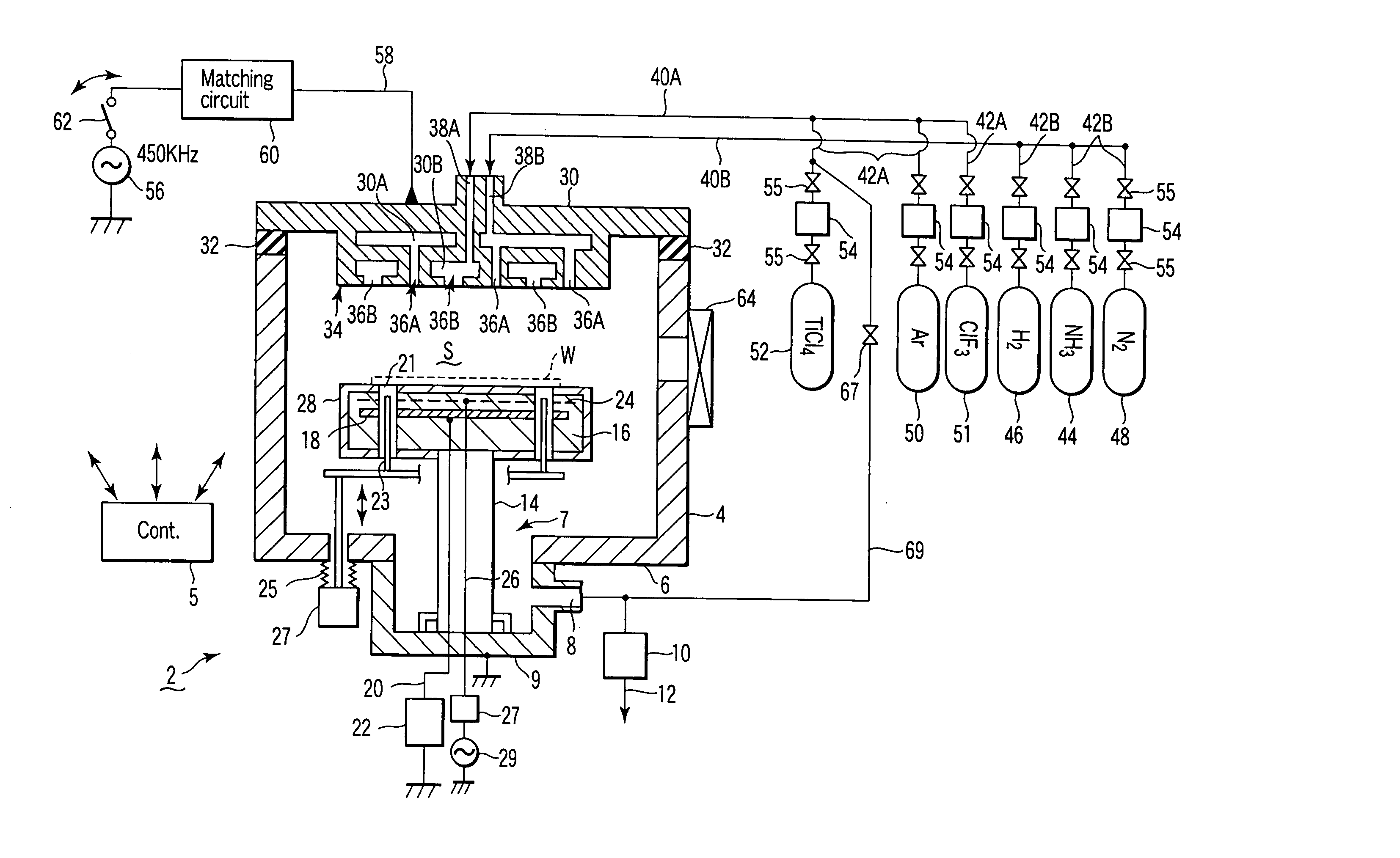
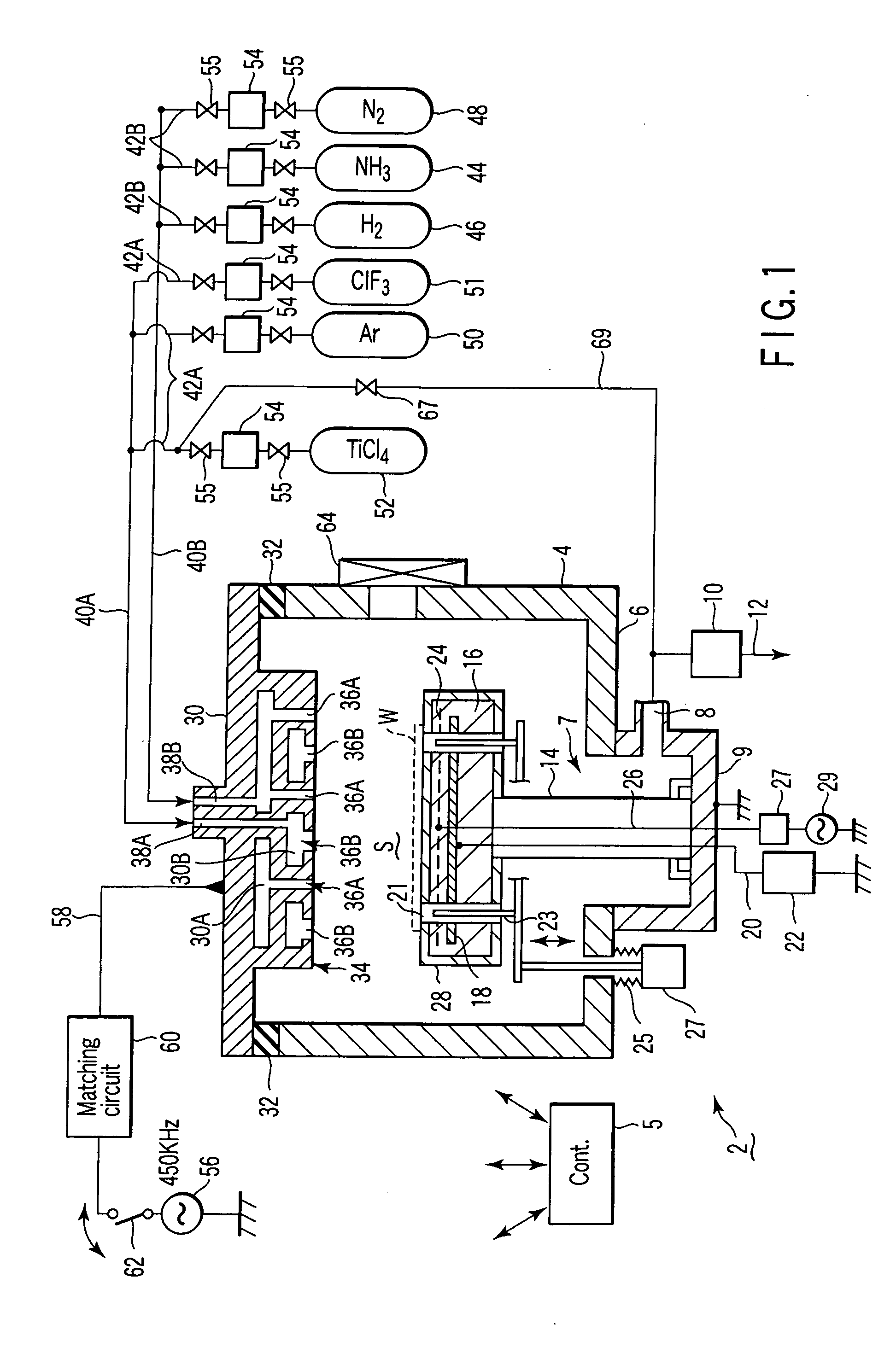
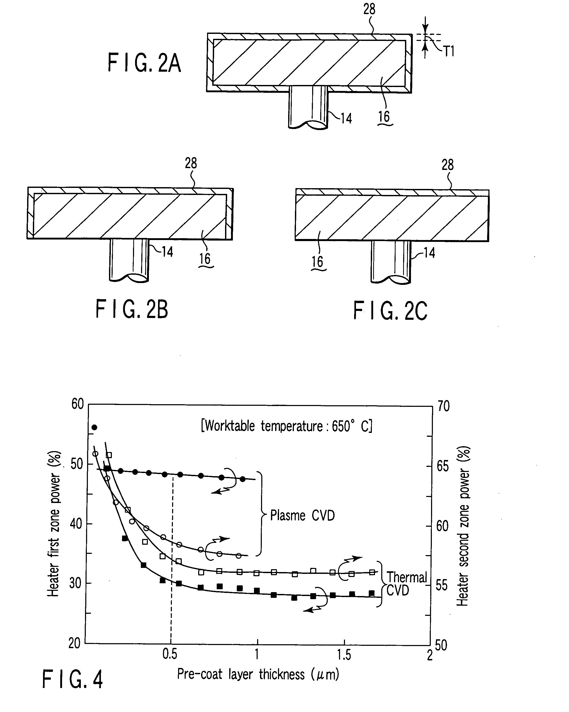
[0068]FIG. 1 is a structural view schematically showing a film formation apparatus for a semiconductor process, according to an embodiment of the present invention. FIGS. 2A to 2C are sectional views respectively showing worktables each with a pre-coat layer formed thereon. In this embodiment, an explanation will be given of a case where a pre-coat layer consisting of a TiN-containing film is formed by plasma CVD and a nitridation process, or thermal CVD.

[0069] As shown in FIG. 1, the processing apparatus 2 includes a cylindrical process container 4 made of, e.g., Al or an Al alloy material. The process container 4 has an opening 7 at the center of the bottom 6, which is airtightly closed by an exhaust chamber 9 protruding downward. The exhaust chamber 9 has an exhaust port 8 formed on one sidewall and connected to an exhaust system 12 including a vacuum pump 10, so that the atmosphere within the container can be exhausted. With this arrangement, the interior of the process contain...

second embodiment

[0125] In the embodiment described above, a pre-coating process is performed to stabilize the state inside the process container 4, immediately after a cleaning process is performed for the interior of the process container 4, or immediately before a wafer is loaded after the processing apparatus 2 undergoes an idling operation. In this case, it has been found that some problem arise if the pre-coating process comprises a Ti film formation process by plasma CVD and a nitridation process by plasma (particularly the cases shown in FIGS. 3A and 3D). Specifically, there is a case where the film quality is deteriorated by local electrical discharge damage on the first wafer subsequently loaded.

[0126] This electrical discharge is thought to be caused by the following mechanism. FIGS. 9A and 9B are explanatory diagrams showing the cause of electrical discharge occurring between a semiconductor wafer and a worktable. Specifically, as shown in FIG. 9A, when a Ti film is formed on the workta...


PUM

PropertyMeasurementUnit
thicknessaaaaaaaaaa
thicknessaaaaaaaaaa
melting pointaaaaaaaaaa

Abstract

A worktable device is disposed inside a film formation process container for a semiconductor process. The worktable device includes a worktable including a top surface to place a target substrate thereon, and a side surface extending downward from the top surface, and a heater disposed in the worktable and configured to heat the substrate through the top surface. A CVD pre-coat layer covers the top surface and the side surface of the worktable. The pre-coat layer has a thickness not less than a thickness which substantially saturates the amount of radiant heat originating from heating of the heater and radiated from the top surface and the side surface of the worktable.

Description

CROSS-REFERENCE TO RELATED APPLICATIONS [0001] This is a Continuation-in-Part Application of PCT Application No. PCT / JP03 / 16961, filed Dec. 26, 2003, which was published under PCT Article 21(2) in Japanese. [0002] This application is based upon and claims the benefit of priority from prior Japanese Patent Applications No. 2003-024264, filed Jan. 31, 2003; and No. 2003-199377, field Jul. 18, 2003, the entire contents of both of which are incorporated herein by reference.BACKGROUND OF THE INVENTION [0003] 1. Field of the Invention [0004] The present invention relates to a worktable device, film formation apparatus, and film formation method for a semiconductor process. The term “semiconductor process” used herein includes various kinds of processes which are performed to manufacture a semiconductor device or a structure having wiring layers, electrodes, and the like to be connected to a semiconductor device, on a target substrate, such as a semiconductor wafer or a glass substrate use...

Claims


Application Information

Patent Timeline
Patent Type & Authority Applications(United States)
IPC IPC(8): C23C16/44C23C16/458C23C16/46H01L21/00H01L21/285
CPCC23C16/4581H01L21/67109H01L21/28556C23C16/46
Inventor WAKABAYASHI, SATOSHIOKABE, SHINYAMURAKAMI, SEISHIMORISHIMA, MASATOTADA, KUNIHIRO
Owner TOKYO ELECTRON LTD
Why Eureka
Try Eureka