SRAM circuitry

a sram cell, low-power technology, applied in the direction of information storage, static storage, digital storage, etc., can solve the problems of large amount of power wasted, sub-threshold leakage, and increasing leakage current in sub-100 nanometer (nm) vlsi devices, and achieve fast “all nmos" and low leakage current

Active Publication Date: 2005-11-24
ANALOG DEVICES INC
View PDF3 Cites 26 Cited by
  • Summary
  • Abstract
  • Description
  • Claims
  • Application Information

AI Technical Summary

Benefits of technology

[0013] The SRAM cells of the present invention have the advantages of (i) being very fast, on the order of 100 pS for a read on a 0.18 μm CMOS; (ii) needing no VDD or VSS wires, as retention power is taken from the bit and wordlines; (iii) having low leakage current thr

Problems solved by technology

Leakage current in sub-100 nanometer (nm) VLSI devices is becoming an increasing problem with each generation.
At such a small scale, the transistors have problems ‘turning off’ (because the threshold voltage Vth is reduced, which increases sub-threshold current) and most CMOS circuits including SRAM and static logic will leak cur

Method used


Image

  • SRAM circuitry
  • SRAM circuitry
  • SRAM circuitry

Examples


Embodiment Construction
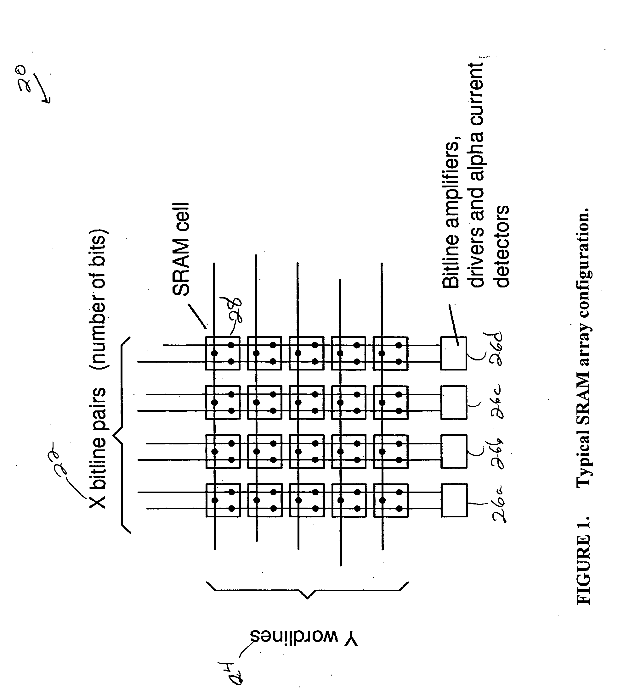
Array Blocks

[0022] Arrays 20 are built up in the X direction 22 to make the memory wider, and in the Y direction 24 by adding more wordlines. The bitlines 22 are commoned. An array 20 of SRAM cell shown in FIG. 1 together with the Wordline drivers and the bitline amplifiers 26a-d completes an X*Y array 20.

Multiple Blocks

[0023] Multiple array blocks would ordinarily be deployed. This helps in several ways. It makes redundancy easier to implement on the array level. It makes access time faster on smaller, less capacitive arrays. The circuits in the individual blocks need only be matched to the local CMOS PVT process conditions on that part of the die. It eases matching requirements etc.

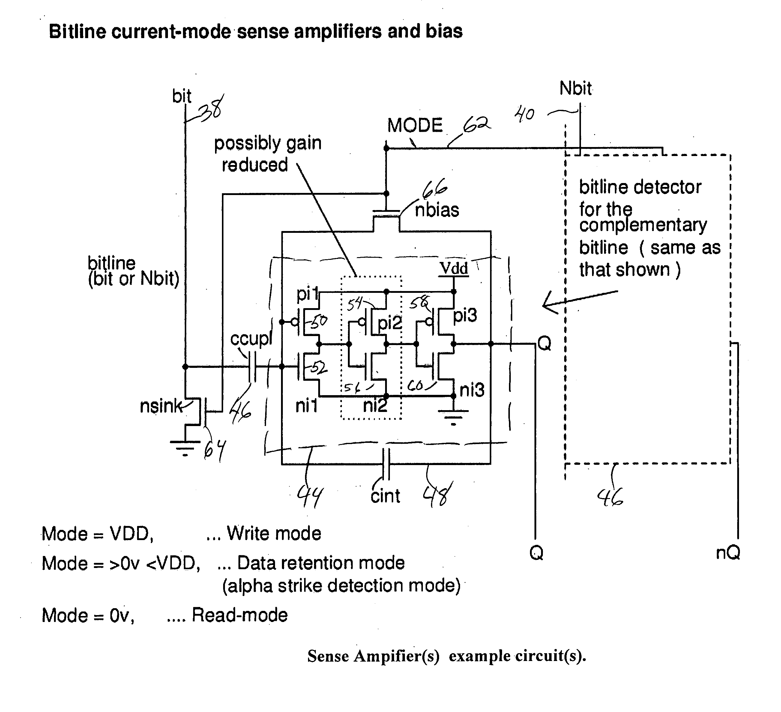
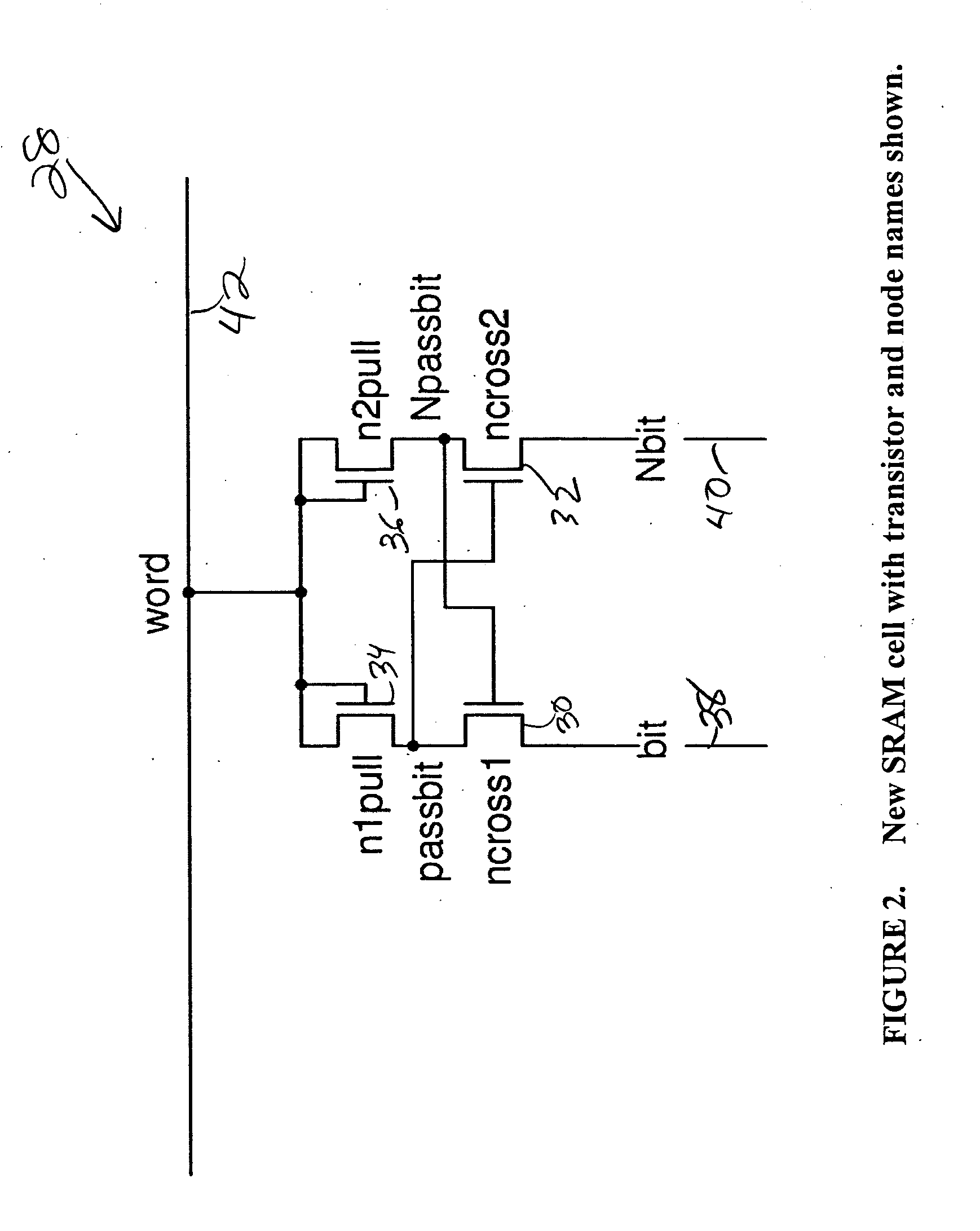
New SRAM Cell And Drive Circuits

[0024] The circuit here aims to give all the benefits associated with the above approaches but in a much simpler way with less overhead in terms of area and delay. It should be noted that the circuit is drawn using NFET transistors, although PFETs could be used in...


PUM


Abstract

A static ram cell is described. The cell includes a pair of cross-coupled transistors and a pair of diode-connected transistors operated from a wordline that provides power to the cell. The cell has three main operating modes, reading, writing and data retention. Reading is performed by sensing current flowing from a powered up wordline through a conductive one of the cross-coupled transistors. Writing is performed by pulsing the source of the conductive one of the cross-coupled transistors with a positive voltage to flip the conductive states of the cross-coupled transistors. Data retention is performed by using leakage currents to retain the conductive states of the cross-coupled transistors. A decoder for an array of static ram cells may be operated synchronously and in a pipelined fashion using a rotary traveling wave oscillator that provides the clocks for the pipeline. The cell capable of detecting an alpha particle strike with suitable circuitry.

Description

CROSS-REFERENCE To RELATED APPLICATIONS [0001] This application claims priority to and incorporates by reference into the instant application Great Britain Application titled “SRAM04,” having patent application number GB0409728.3, filed May 4, 2004. FIELD OF THE INVENTION [0002] This invention relates generally to SRAM cells and more particularly to a high speed, low power SRAM cell. DESCRIPTION OF THE RELATED ART [0003] Leakage current in sub-100 nanometer (nm) VLSI devices is becoming an increasing problem with each generation. At such a small scale, the transistors have problems ‘turning off’ (because the threshold voltage Vth is reduced, which increases sub-threshold current) and most CMOS circuits including SRAM and static logic will leak current from VDD to GND through P- and N-channel transistors. These currents are in the order of 25 nA per transistor pair. With possibly 1 billion transistors on a chip, the amount of power wasted can be large. Sub-threshold leakage increases...

Claims


Application Information

Patent Timeline
IPC IPC(8): G11C11/00G11C11/412
CPCG11C11/4125G11C11/412
Inventor WOOD, JOHN
Owner ANALOG DEVICES INC
Why Eureka
Try Eureka