Eureka AIR delivers breakthrough ideas for toughest innovation challenges, trusted by R&D personnel around the world.

Forming a conductor circuit on a substrate

Inactive Publication Date: 2005-11-24
YISSUM RES DEV CO OF THE HEBREW UNIV OF JERUSALEM LTD
View PDF6 Cites 6 Cited by
  • Summary
  • Abstract
  • Description
  • Claims
  • Application Information

AI Technical Summary

Benefits of technology

[0006] The substrate may be made of a pliable or flexible material or may be made of a rigid material. The substrate material may be porous, e.g. made of paper or cloth; the substrate may only have a porous surface formed or attached to a non-porous material; or may be made entirely of a non-porous material. A porous surface is preferred for some applications as it permits the

Problems solved by technology

The production of PCBs, by a variety of patterning techniques, is a time-consuming procedure, involving the use of noxious chemicals, particularly those needed for copper etching.
The use of such chemicals adds costs and complexity to the procedure in view of the special disposal requirements of such chemicals.

Method used


Image

  • Forming a conductor circuit on a substrate
  • Forming a conductor circuit on a substrate
  • Forming a conductor circuit on a substrate

Examples


example

Pd-Nanoparticles:

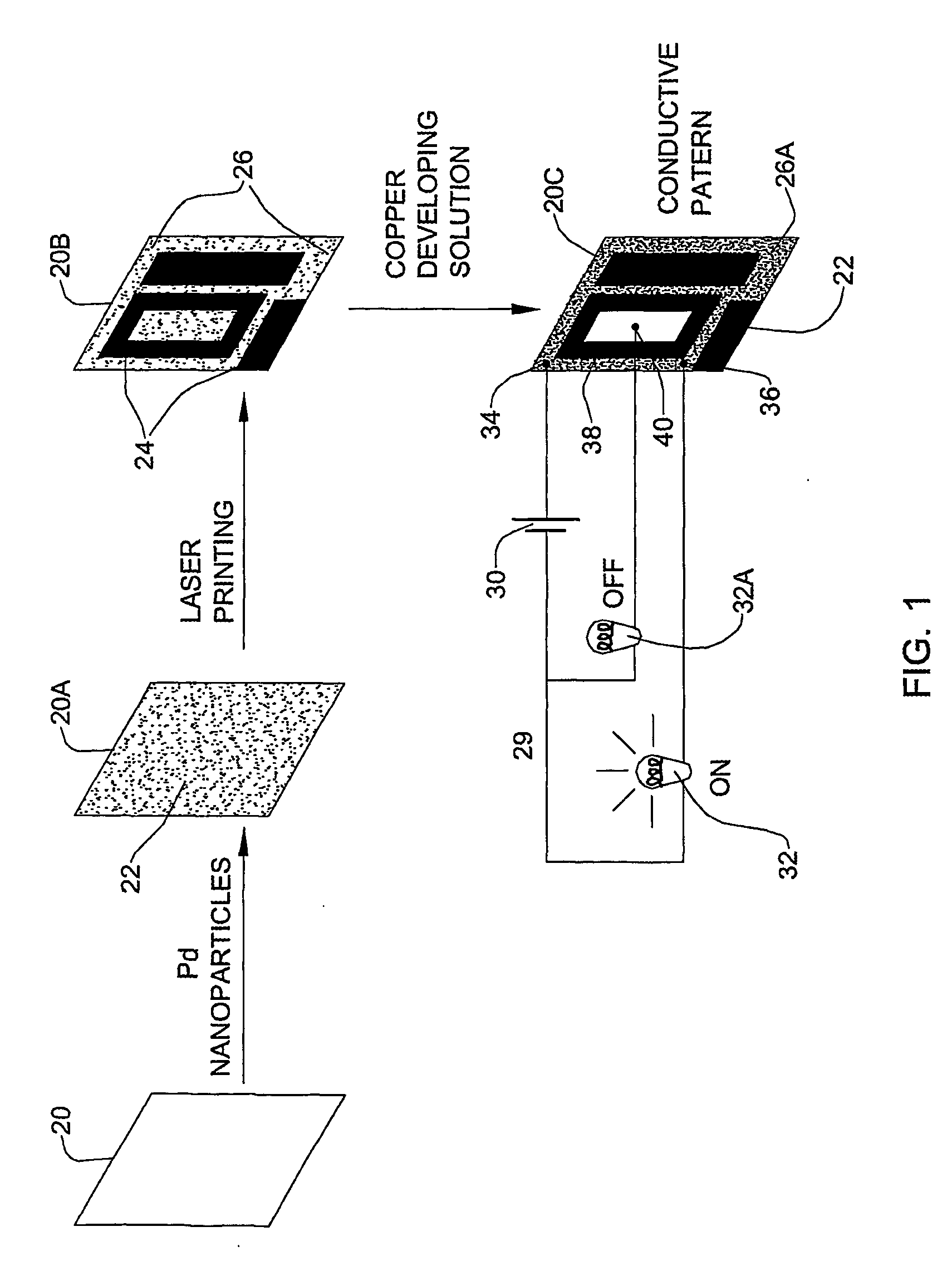
[0045] Palladium nanoparticles were synthesized according to a literature procedure (P. C. hidber, W. Helbig, E. Kim, G. M. Whitesides, Langmuir, 12:1375-1380, 1996). Palladium (II) acetate (0.5 g, 2.23 mmol) and tetraoctadecylammonium bromide (625 mg, 0.56 mmol) were suspended in a mixture of toluene (20 mL) and THF (4 mL). Ethanol (3 mL) was added, then the mixture was stirred at reflux for 15 hours. After the reaction was cooled, ethanol (20 mL) was added and the nanoparticles were left for 24 hours to precipitate. The supernatant was decanted, then further ethanol (50 mL) was added, the nanoparticles were allowed to settle, and the supernatant was again decanted. The remaining slurry was dried under vacuum.

Pd-Treatment of the Paper:

[0046] Ordinary white laser printer paper was used. The dry Pd nanoparticles were dissolved in toluene at a concentration of 10 mg mL−. This solution was sprayed on the paper at approximately 1 mL per 100 cm2 (i.e. at a Pd-densit...


PUM

PropertyMeasurementUnit
Diameteraaaaaaaaaa
Electrical conductoraaaaaaaaaa

Abstract

Disclosed is a process for forming a conductor pattern on a face of a substrate, which is typically sorbing and porous, such as paper or cloth. The method comprises forming on the surface an exposed pattern of colloid particles, corresponding to the conductor pattern to be formed. The colloid particles suitable for use according to the invention are those that are capable of catalyzing electroless deposition of copper, silver, gold, and the like. After the exposed pattern of colloid particles is formed, precipitation of a metal substance on said face is caused, to form said conductor pattern.

Description

FIELD AND BACKGROUND OF THE INVENTION [0001] The present invention concerns a method for forming a conductor pattern on a substrate. [0002] Printed circuit boards (PCBs) are solid, rigid or flexible substrates with a conduction circuit printed thereon. The production of PCBs, by a variety of patterning techniques, is a time-consuming procedure, involving the use of noxious chemicals, particularly those needed for copper etching. The use of such chemicals adds costs and complexity to the procedure in view of the special disposal requirements of such chemicals. SUMMARY OF THE INVENTION [0003] In the following, the term “conductor pattern” will be used to denote the conductor arrangement on the face of a substrate. This conductor pattern in fact defines the electrical conductivity between different portions of the substrate. For example, from one point of the substrate connected to one electronic component to another point which is connected to another component, to a current source, t...

Claims


Application Information

Patent Timeline
IPC IPC(8): C23C18/16C23C18/31H05K3/10C23C18/18H05K3/18H05K3/46
CPCH05K3/102C23C18/30C23C18/1644C23C18/1608
Inventor SHIPWAY, ANDREWWILLNER, ITAMAR
Owner YISSUM RES DEV CO OF THE HEBREW UNIV OF JERUSALEM LTD
Why Eureka
Eureka Blog
Learn More