
Electron emission device including conductive layers for preventing accumulation of static charge

a technology of conductive layers and electron emission devices, which is applied in the manufacture of electric discharge tubes/lamps, tubes with screens, discharge tubes luminescnet screens, etc., can solve problems such as abnormal operation, arcing flashover, and failure of devices, and increase the number of structural components and therefore the cost of production

Inactive Publication Date: 2005-12-01
SAMSUNG SDI CO LTD
View PDF1 Cites 6 Cited by
  • Summary
  • Abstract
  • Description
  • Claims
  • Application Information

AI Technical Summary

Benefits of technology

[0011] In one exemplary embodiment of the present invention, there is provided an electron emission device which prevents the static charges from being accumulated on the insulating layer without introducing a separate driving IC.

Problems solved by technology

As a result of this structure, static charges are accumulated on the insulating layer of conventional electron emission devices in the non display areas and cause device failures such as abnormal operation, arcing, and flashover.
In conventional techniques, including the ion shield technique explained above, because the ion shield layer receives its driving voltage from an IC separate from the IC used for driving the emission electrode, the number of structural components and therefore the cost of production, are increased.

Method used


Image

  • Electron emission device including conductive layers for preventing accumulation of static charge
  • Electron emission device including conductive layers for preventing accumulation of static charge
  • Electron emission device including conductive layers for preventing accumulation of static charge

Examples


Embodiment Construction

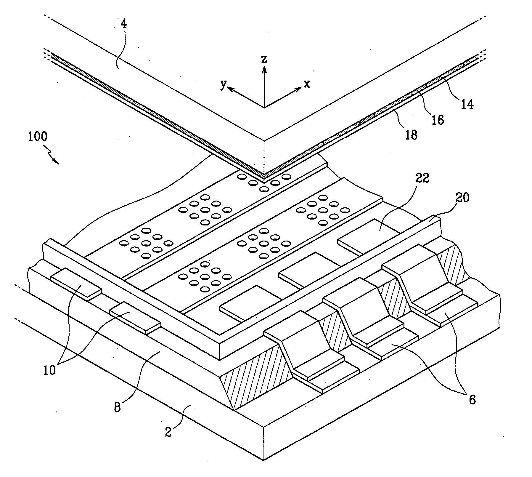
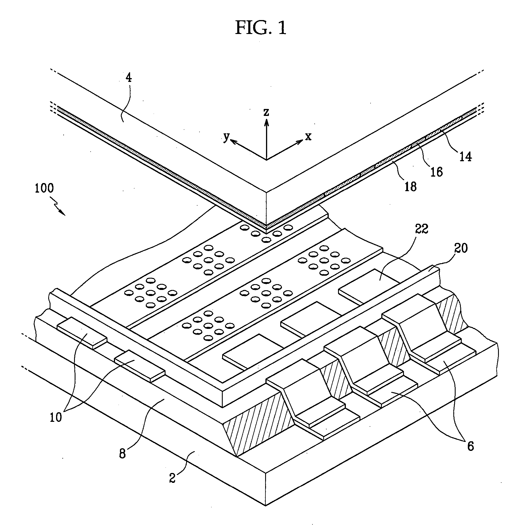
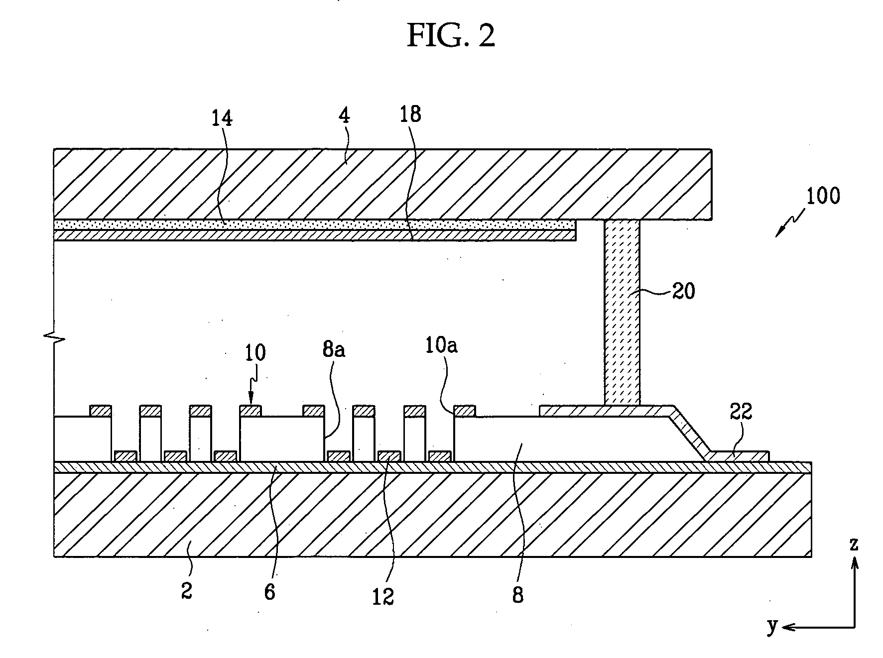
[0021] As seen in FIG. 1, in one embodiment the electron emission device 100 includes first substrate 2 and second substrate 4 parallel to each other. The substrates 2, 4 are assembled by attaching them to each other via a sealing member 20 leaving a distance in between the substrates 2, 4. The inner space between the substrates 2, 4 is exhausted to be in a partial vacuum state hence creating a vacuum chamber between the substrates.

[0022] As a set of first electrodes, a number of cathode electrodes 6 are formed, in a stripe pattern, on the first substrate 2. Stripes of cathode electrodes 6 are spaced apart from one another and are formed, for example, along the y-axis of the drawing in FIG. 1. An insulating layer 8 is formed on the surface of the first substrate 2 covering the cathode electrodes 6. A number of gate electrodes 10 are formed on the insulating layer 8, in another stripe pattern, as a set of second electrodes. Stripes of gate electrodes 10 are spaced apart from one ano...


PUM


Abstract

An electron emission device with conductive layers for preventing accumulation of static charges on an insulating layer of the device is shown that does not require an independent driving circuit. The device includes cathode electrodes formed on a substrate and separated from gate electrodes by an insulating layer formed over the cathode electrodes, all inside a partial vacuum chamber. Crossings of cathode and gate electrodes form the display areas while in the non-display areas of the insulating layer, that are susceptible to accumulation of electrostatic charge, conductive layers are formed parallel to the cathode or gate electrodes, for the most part separated from these electrodes by the insulating layer. Outside the device chamber, the conductive layers are electrically coupled to their corresponding electrodes. Conductive layers thus formed and coupled discharge accumulated static charge over the insulating layers inside the device to the outside circuit.

Description

CROSS REFERENCE TO RELATED APPLICATION [0001] This application claims priority to and the benefit of Korean Patent Application No. 10-2004-0038989 filed on May 31, 2004 in the Korean Intellectual Property Office, the entire content of which is incorporated herein by reference. BACKGROUND OF THE INVENTION [0002] 1. Field of the Invention [0003] The present invention relates to an electron emission device, and in particular, to an electron emission device which has an electrode structure for preventing the electrostatic charges from being accumulated on the insulating layer. [0004] 2. Description of Related Art [0005] Generally, electron emission devices are classified into a first type where a hot cathode is used as an electron emission source, and a second type where a cold cathode is used as the electron emission source. The cold cathode electron emission devices, in turn, include field emitter array (FEA) devices, surface conduction emitter (SCE) devices, metal-insulator-metal (MI...

Claims


Application Information

Patent Timeline
IPC IPC(8): H01J1/304H01J1/02H01J1/30H01J3/02H01J29/48H01J31/12
CPCH01J1/30H01J31/127H01J29/481H01J3/021
Inventor HWANG, SEONG-YEON
Owner SAMSUNG SDI CO LTD
Learn More