Resistor and switch-minimized variable analog gain circuit

Inactive Publication Date: 2005-12-01
LANTIQ BET GMBH & CO KG
View PDF3 Cites 14 Cited by
  • Summary
  • Abstract
  • Description
  • Claims
  • Application Information

AI Technical Summary

Benefits of technology

[0009] The benefit of resistor miniaturization by using relatively low value resistors is especially useful in technologies where resistors having high values are not easily implemented. For example, in DSM processes, h

Problems solved by technology

For example, in DSM processes, high she

Method used


Image

  • Resistor and switch-minimized variable analog gain circuit
  • Resistor and switch-minimized variable analog gain circuit
  • Resistor and switch-minimized variable analog gain circuit

Examples


Example

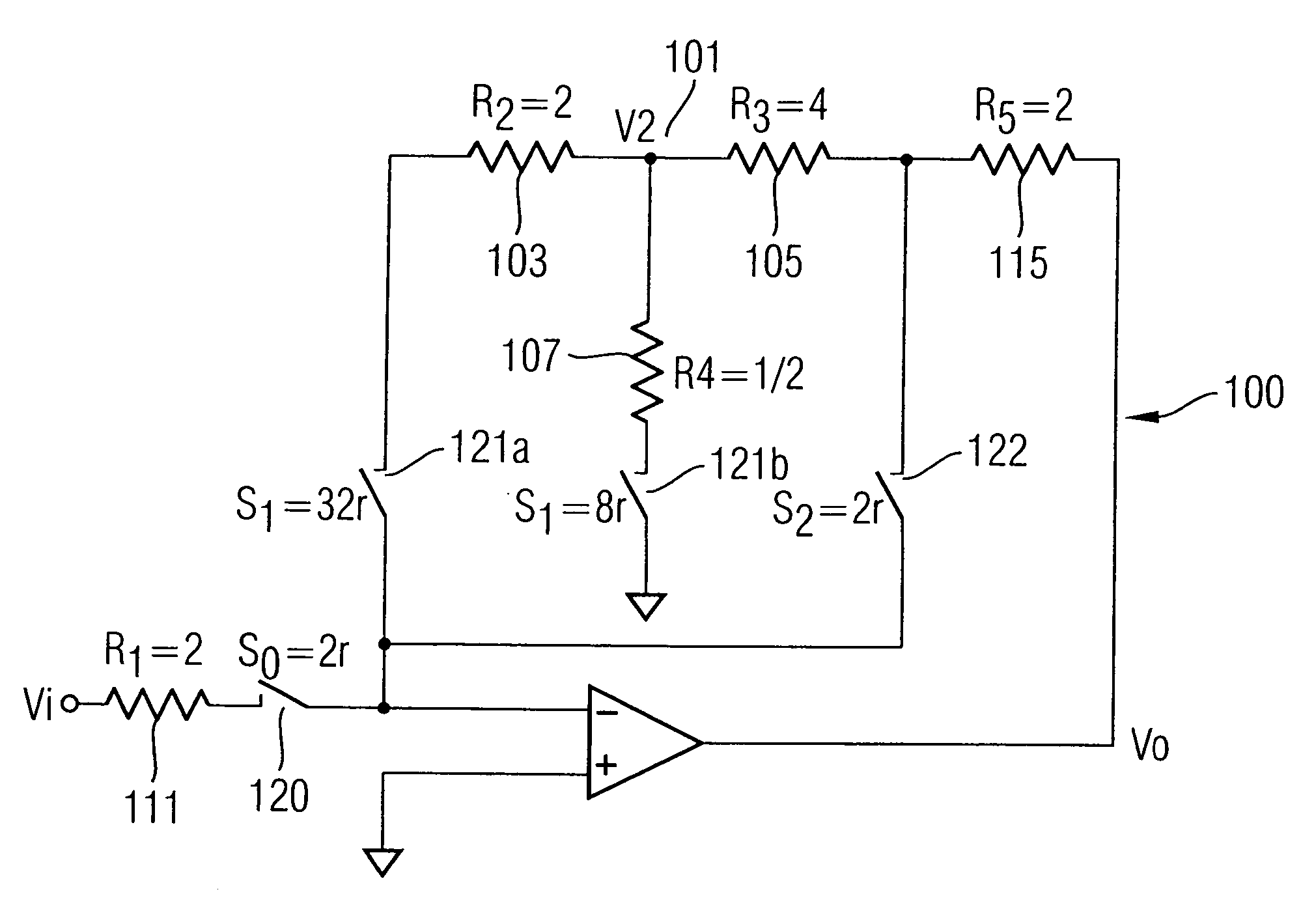
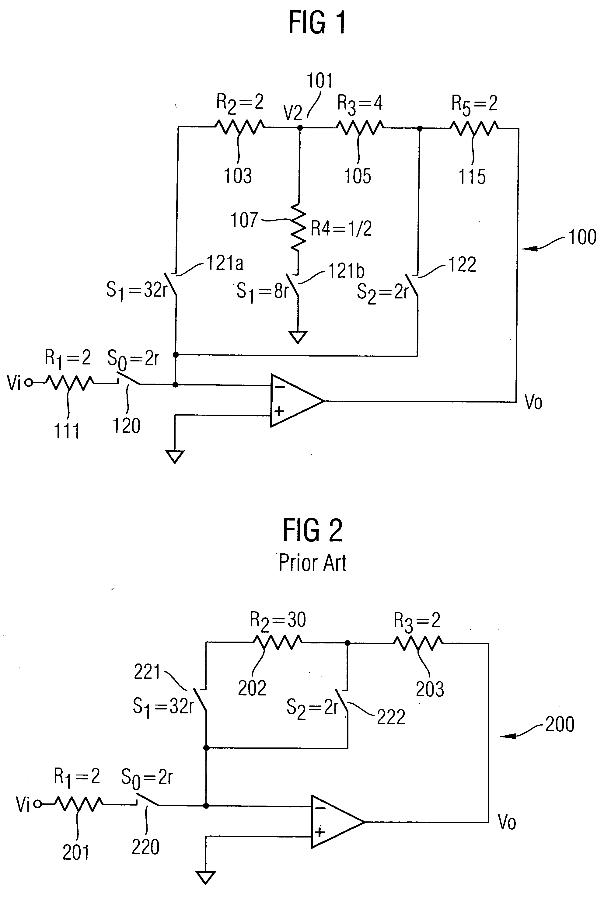
[0024]FIG. 1 shows a gain step circuit 100 in accordance with one embodiment of the present invention. The resistor efficient gain step circuit reduces the resistor area without adversely affecting the functionality of the circuit. The present invention may also be applied to a normal gain circuit where there is no selection of gain. Although the gain step circuit illustrated in FIG. 1 supports both 0 dB and 24 dB gains, the present invention can also be applied to provide circuits with other gain values.

[0025] Generally, the present invention minimises the resistance of the resistors used by replacing the large resistors in a conventional gain circuit with a T resistor network. For example, the inventive gain circuit in FIG. 1 is derived by replacing the large resistor R2202 in the conventional gain step circuit of FIG. 2 with a T resistor network 101 comprising three resistors R2103, R3105, R4107. A T resistor network is made up of three branches wherein one end of each branch is...


PUM


Abstract

A DSM variable high-gain circuit includes a differential amplifier and a negative feedback loop comprising low resistance poly resistors and switches configured in a T-structure having a junction point as part of the negative feedback loop. A third resistor branch of the T-structure includes a switch that connects the junction point through the third resistor branch to ground when in a closed state and that turns the third resistor branch into an open circuit when in an open state The switch of the third resistor branch, when in the closed state, produces a gain at the output of the variable high-gain circuit.

Description

FIELD OF THE INVENTION [0001] The present invention relates to gain circuits and in particular to gain circuits fabricated using deep sub-micron processes. BACKGROUND OF THE INVENTION [0002] Resistors with high resistance values are often used in the implementation of analog circuitry. Providing resistors with high resistance values was not a problem in earlier technologies as high sheet resistance resistors were available from the standard process flow. However, with the scaling down of critical dimensions in state of the art CMOS technologies high sheet resistance resistors are typically not available. For example, in a typical 0.18 micron technology, the poly resistors generated from a conventional process flow have a low sheet resistance ranging from 200 to 400 ohms per square. In order to obtain high sheet resistance resistors, additional process steps and mask levels are required. This is undesirable as it adds to the complexity and cost of fabricating the ICs. [0003] As a res...

Claims


Application Information

Patent Timeline
IPC IPC(8): H03G1/00H03G3/30
CPCH03G1/0088
Inventor MA, FAN YANGYU, WEN
Owner LANTIQ BET GMBH & CO KG
Why Eureka
Try Eureka