Luminance enhancement apparatus and method

a technology of luminance and apparatus, applied in the field of illumination, can solve the problems of reducing the efficiency of an oled, and reducing the ratio of converted light to incident light, and achieve the effect of enhancing luminan

Inactive Publication Date: 2005-12-01
KONINKLIJKE PHILIPS ELECTRONICS NV
View PDF15 Cites 111 Cited by
  • Summary
  • Abstract
  • Description
  • Claims
  • Application Information

AI Technical Summary

Benefits of technology

[0024] In accordance with another aspect of the present invention, there is provided a method for enhancing luminance produced by one or more point light sources, said method comprising the steps of: providing the one or more point light sources, each comprising a light-emitting element that serves as a primary source of electromagnetic radiation and includes a conversion system for changing one or more wavelengths of the electromagnetic radiation to one or more alternate wavelengths of electromagnetic radiation; and forming a predetermined surface relief pattern on a face of the conversion system, said face being opposite the light-emitting element.

Problems solved by technology

However, this process may not be completely efficient in that some of the blue light may be absorbed and converted into thermal energy.
A further problem may occur when the phosphor particles become “saturated”, wherein for example a further increase in excitation light does not produce a corresponding increase in converted light.
All of these effects tend to decrease the efficiency of an OLED, where the efficiency is defined as the ratio of optical output power, which is measured in lumens, to the electrical input power which is measured in watts.
Therefore the ratio of converted light to the incident light is limited by the maximum possible density of the phosphorescent materials.
As a result, these films increase the luminance or “photometric brightness” of the underlying light source in a direction substantially normal to the film, however they typically decrease the luminance at off-axis viewing angles.
However, an optimal angle for a phosphor or other conversion layer that may be self-excited by its emitted light, is not considered in this patent.
In addition, this patent does not consider the advantages of an area light source in physical contact with the substrate without an intervening air gap therebetween.

Method used


Image

  • Luminance enhancement apparatus and method
  • Luminance enhancement apparatus and method
  • Luminance enhancement apparatus and method

Examples


Embodiment Construction

Definitions

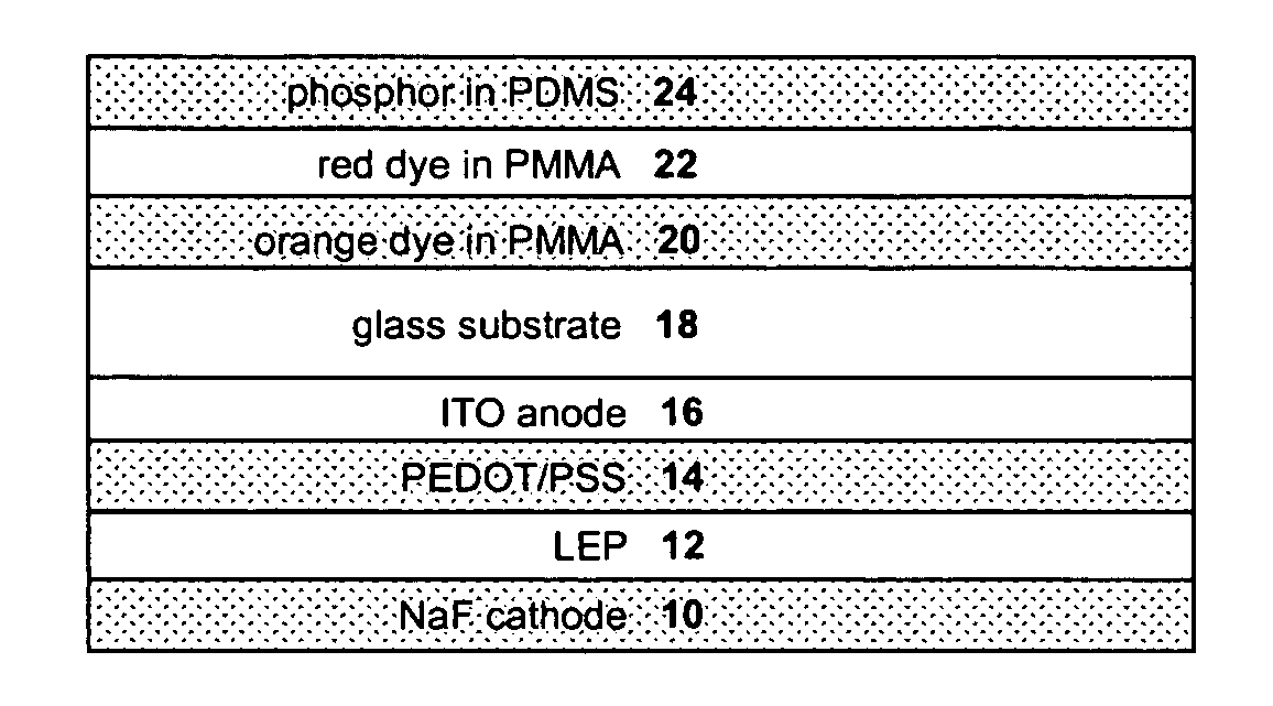
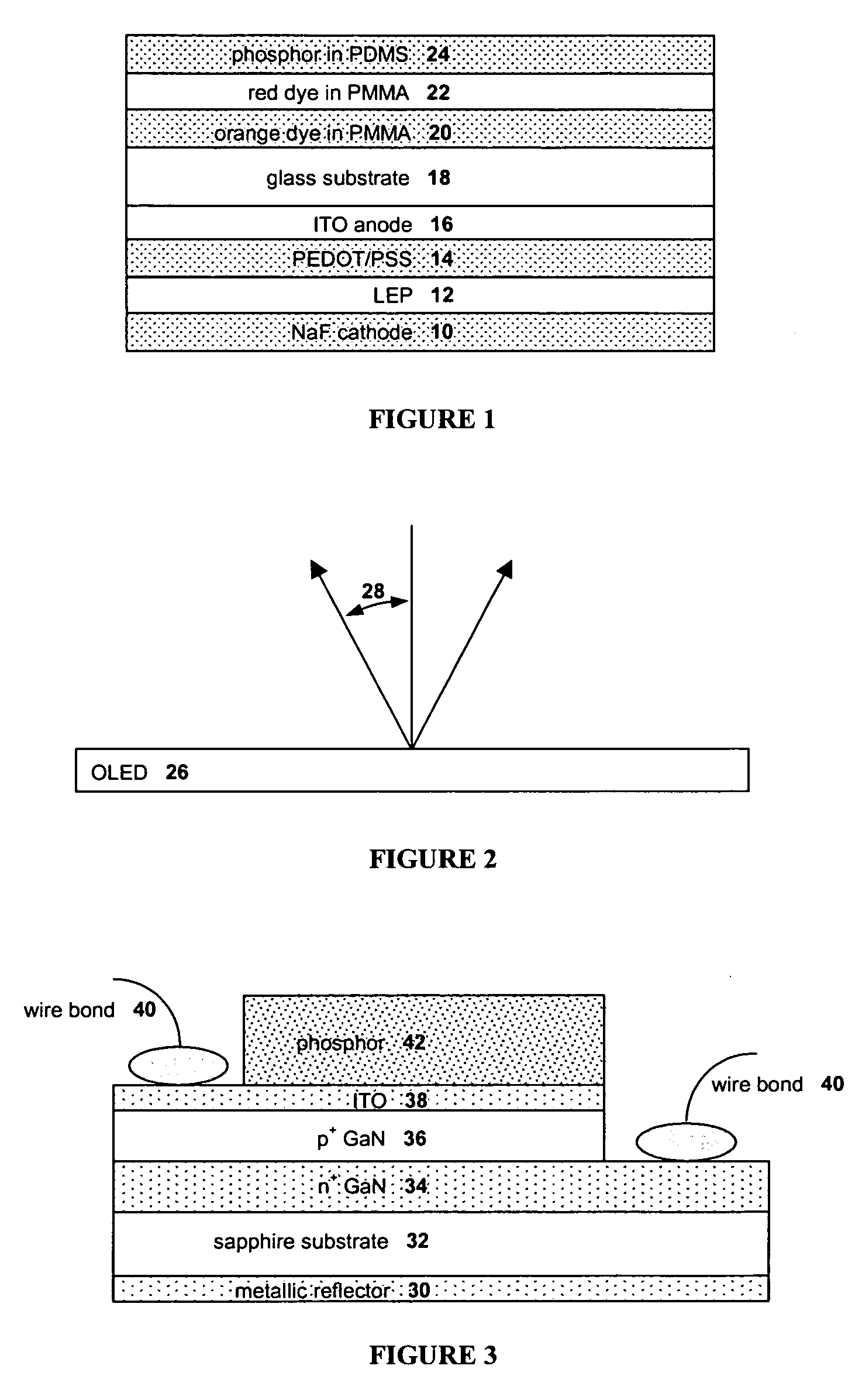
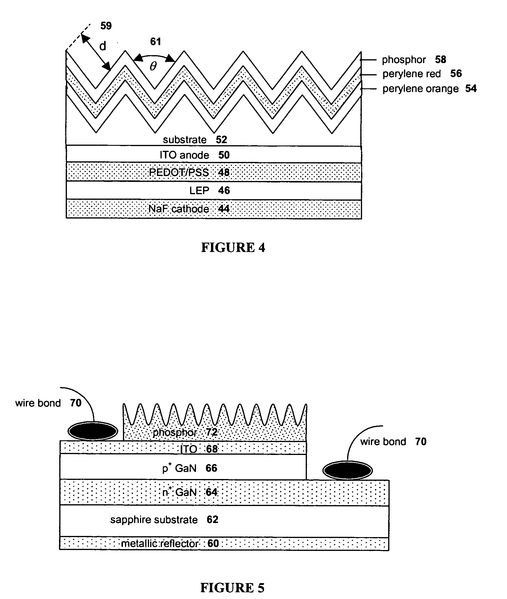
[0039] The term “light-emitting element” is used to define any device that emits radiation in the visible region, or any other region of the electromagnetic spectrum, when a potential difference is applied across it or a current is passed through it, for example, a semiconductor or organic light-emitting diode, quantum dot light-emitting diode, polymer light emitting diode or other similar devices as would be readily understood.

[0040] Unless defined otherwise, all technical and scientific terms used herein have the same meaning as commonly understood by one of ordinary skill in the art to which this invention belongs.

[0041] The present invention provides a luminance enhancement apparatus and method for use with light-emitting elements comprising a conversion system adjacent to the light-emitting element for converting electromagnetic radiation of one or more wavelengths to alternate wavelengths. This conversion process can be enabled by the absorption of radiation wit...


PUM

PropertyMeasurementUnit
angleaaaaaaaaaa
angleaaaaaaaaaa
angleaaaaaaaaaa

Abstract

The present invention provides a luminance enhancement apparatus and method for use with light-emitting elements comprising a conversion system adjacent the light-emitting element for converting electromagnetic radiation of one or more wavelengths to alternate wavelengths. This conversion process can be enabled by the absorption of the one or more wavelengths by the conversion system and emission of the alternate wavelengths thereby. The conversion system comprises a predetermined surface relief pattern on the face opposite the light-emitting element to provide a means for reducing absorption of the emitted alternate wavelengths in addition to providing a means for reflection of the emitted alternate wavelengths from the conversion system with a reduced number of reflections, thereby enhancing the illumination provided by the light-emitting element. As the present invention operates on principles of increased surface area and self-excitation of the conversion materials through the use of a predetermined surface relief pattern, the present invention may be applied to both organic LEDs, phosphor-coated semiconductor LEDs, and light-emitting elements coated with a population of quantum dots embedded in a host matrix.

Description

CROSS-REFERENCE TO RELATED APPLICATION [0001] This application claims the benefit under 35 U.S.C. § 119(e) of U.S. Provisional Application No. 60 / 574,950, filed May 28, 2004, and entitled “Luminance Enhancement Apparatus and Method”, which is hereby incorporated by reference herein in its entirety.FIELD OF THE INVENTION [0002] The present invention field of illumination and in particular to apparatus and methods of enhancing the luminance from light-emitting elements. BACKGROUND [0003] There are a number of light-emitting elements with these including semiconductor light-emitting devices, organic light-emitting devices and others as would be readily understood. For example, organic light-emitting devices (OLEDs) comprise thin layers of organic materials deposited on a substrate that when excited by the flow of electrical current, emit visible light. Such devices can be useful in applications such as displays for cellular telephones, personal digital assistants, flat-screen televisio...

Claims


Application Information

Patent Timeline
Patent Type & Authority Applications(United States)
IPC IPC(8): F21V11/00G02F2/02H01L33/50H01L51/50H01L51/52H01S3/10H05B33/22
CPCB82Y10/00B82Y20/00H01L51/5271H01L51/52H01L51/5262H01L51/5036H01L2224/49107H10K50/125H10K50/80H10K50/85H10K50/856H10K2102/331
Inventor ASHDOWN, IAN
Owner KONINKLIJKE PHILIPS ELECTRONICS NV
Why Eureka
Try Eureka