Optical coupling device

a coupling device and optical technology, applied in the field of optical coupling devices, can solve the problems of limiting the ability of the communications industry to realize the full potential of optical carrier frequencies, and a key source of loss, so as to achieve efficient transmission of optical modes and efficient transmission of signals.

Inactive Publication Date: 2005-12-01
ENERGY CONVERSION DEVICES INC
View PDF2 Cites 23 Cited by
  • Summary
  • Abstract
  • Description
  • Claims
  • Application Information

AI Technical Summary

Benefits of technology

[0013] This invention provides an optical coupling device that efficiently transfers an optical mode from a transmitting optical element to a receiving optical element. The devic

Problems solved by technology

Achievement of THz range communication frequencies has, however, proven to be more challenging than expected as the initial and most of today's optical communication systems are optoelectronic in nature and rely on electronic components (e.g. switches, modulators, controllers, amplifiers, connectors, filters) to control light.
These components introduce an electronic bottleneck that limits the ability of the communications industry to realize the full potential of optical carrier frequencies.
Since the input optical signals received by an integrated optical component are initially introduced into a waveguide, a central issue in the coupling of fibers to planar integrated optical components is the efficient transfer of light from a fiber into a planar waveguide.
The fiber-waveguide junction is a key source of loss in an all-optical system.
The potential for losses in the transformation is high, especially in the fiber to waveguide direction since a large diameter beam needs to be converted to a small diameter beam without substantial loss of power.
Simple end-coupling (back-to-back placement) of a fiber to an integrated waveguide leads to substantial losses due to the large mismatch in cross-sectional area between the fiber and the waveguide.
Much of the signal exiting the fiber is unable to enter the much smaller waveguide due to a mism

Method used


Image

  • Optical coupling device
  • Optical coupling device
  • Optical coupling device

Examples


example 1

[0059] In this example, we consider an embodiment of the instant device that includes two interspersed dielectric materials where the dielectric materials have different permittivities. The device has an input end having an input cross-section and an output end having an output cross-section where the cross-sectional area of the device varies continuously from the input cross-section to the output cross-section along the length of the device. The input and output cross-sections have a cross-sectional area that includes a certain fill factor of one of the dielectric materials and a certain fill factor of the other of the dielectric materials where the fill factors of the two dielectric materials differ in the input and output cross-sections. In a preferred embodiment, the fill factors of the two dielectric materials vary continuously over different cross-sections along a propagation pathway through the device.

[0060] The coupling device in this example interconnects an optical fiber ...

example 2

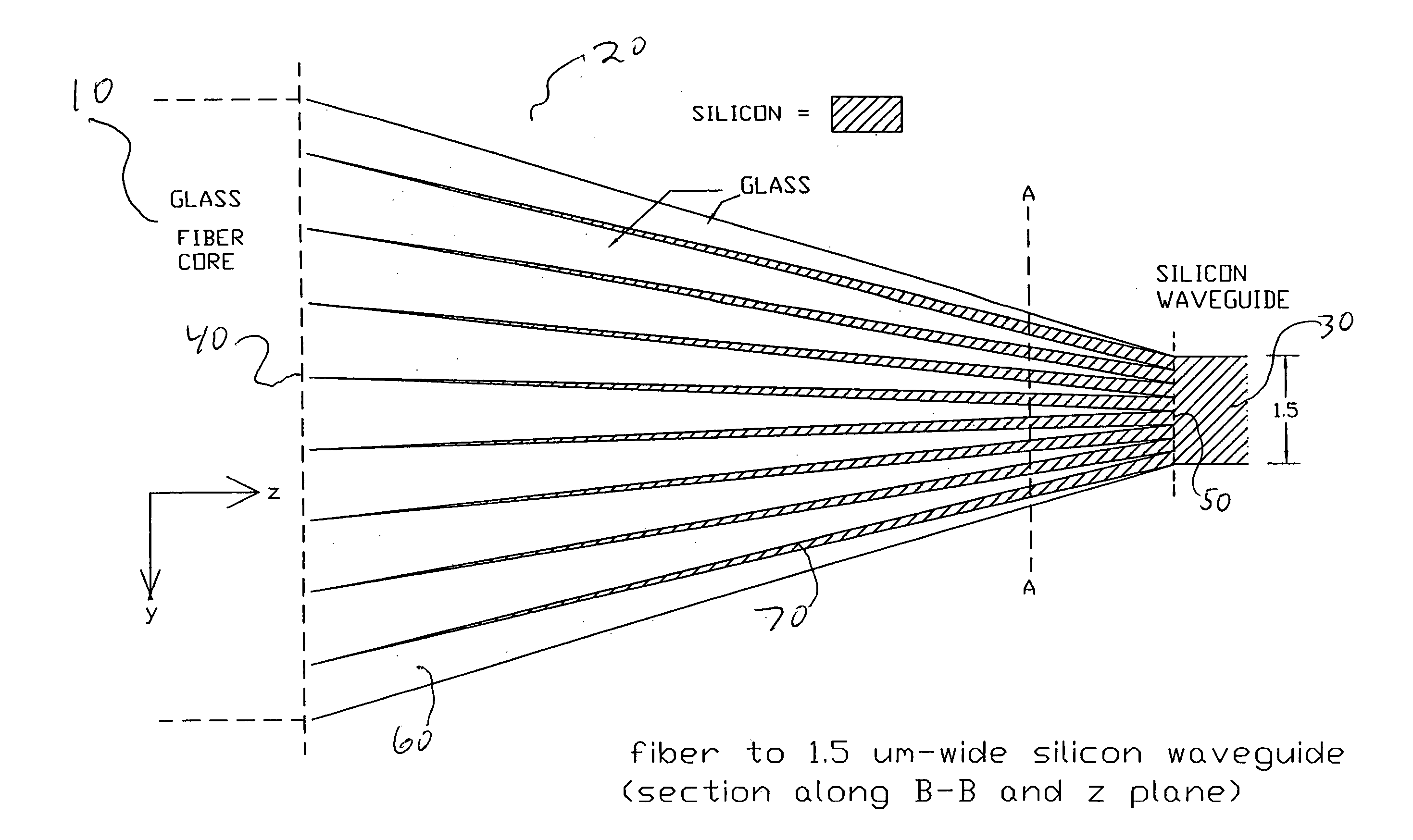
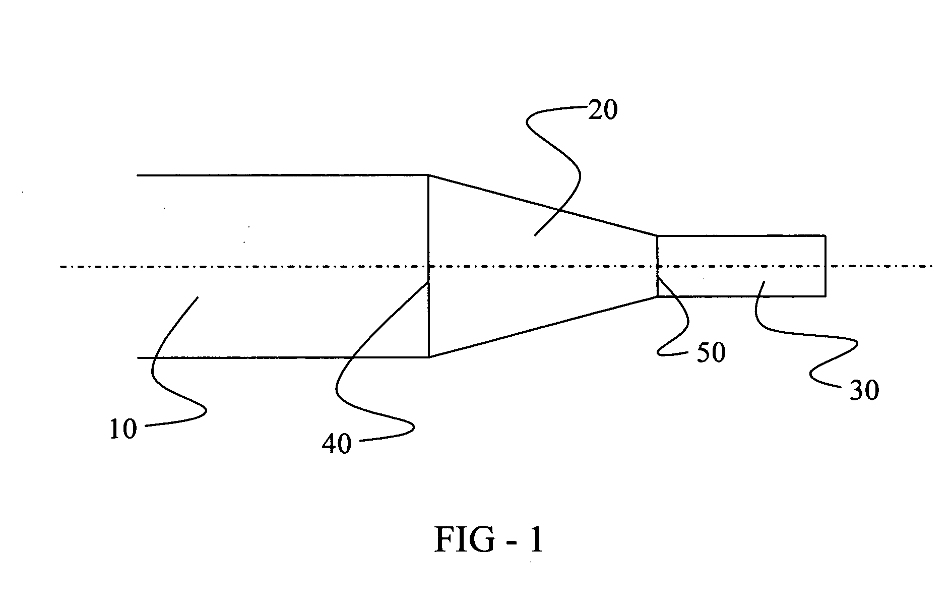
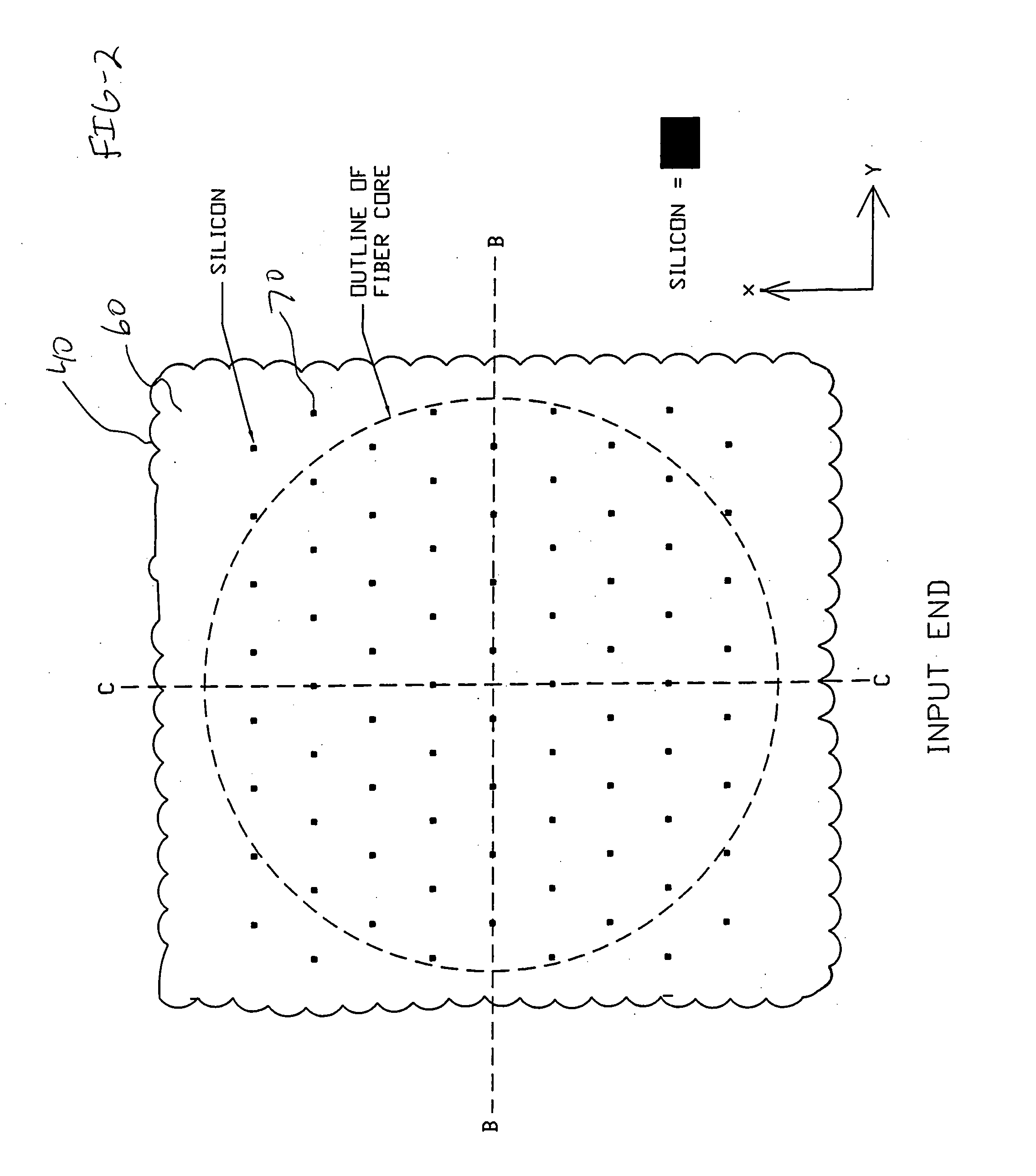
[0069] In this example, a coupling device for a planar integrated optical element is described. The device of this example provides coupling of an optical fiber having a glass core region with a silicon slab waveguide where the central axis of the fiber is not aligned with the central axis of the waveguide. More specifically, the coupling device of this example permits the efficient transfer of an optical signal from a fiber to a waveguide where the fiber and waveguide have a boundary that lie in a common plane. Such a configuration is desirable, for example, in integrated optical elements in which all-planar structures are used. In these structures, individual elements of an optical circuit are deposited or otherwise placed on a common surface and it is desirable to route optical signals from one device to another.

[0070] The optical fiber and silicon waveguide are as described in Example 1 hereinabove and the coupling element of this example includes two dielectric materials: glas...

example 4

[0083] In the foregoing examples, representative input and output cross-sections are shown and conditions relevant to the efficient transfer of an optical signal from a transmitting device to a receiving device via the instant coupling device are described. In this example, the cross-sectional shape of one or more dielectric materials within the instant coupling device in the direction of propagation of the optical signal is considered.

[0084] The conditions described hereinabove for conserving impedance along the length of the coupling device are based on a compensation of effects resulting from the variation in the cross-sectional geometry of the coupling device through tapering to adjust the physical dimensions in which the optical signal is confined from a size comparable to the transmitting device to a size comparable to the receiving device by a compensating change in effective permittivity through a variation in the fill factor of one or more of the constituent dielectric mat...


PUM


Abstract

An optical coupling device for the efficient transfer of an optical signal between optical components. The device can receive an optical signal from a transmitting component connected to its input end and efficiently transmit that signal to a receiving component connected to its output end. The instant device includes a combination of two or more dielectric materials and provides impedance matching at the input and output ends as well as impedance conservation during propagation of the optical signal through the device. Impedance matching at the input and output ends is controlled through variations in the relative proportions of the constituent dielectric materials of the device in the cross-sections of input and output ends to achieve an effective permittivity that closely matches that of the interconnected component. Impedance conservation within the instant device is achieved through simultaneous variations in the cross-sectional shape of the device and cross-sectional fill factors of the constituent dielectric materials. The impedance conditions, in combination with high spatial overlap at the input and output ends, minimize losses in the power of signal transmitted between the interconnected optical components.

Description

FIELD OF INVENTION [0001] This invention pertains to optical coupling devices that interconnect optical elements. The optical coupling devices efficiently transfer light from one optical element to another optical element along an interconnection path. More specifically, this invention pertains to optical coupling devices that integrate two or more optical media in such a way that the cross-sectional area and / or refractive index of the coupling device vary smoothly along an interconnection pathway between optical elements. BACKGROUND OF THE INVENTION [0002] The development of communication systems over time has been central to the progress of human civilization. The evolution of communications has largely been a story of technological evolutions that have served to increase the bandwidth, speed and distance of communications. The era of electronic communications began with Morse's development of the telegraph, a technology that provided instantaneous communication, but at a rate of ...

Claims


Application Information

Patent Timeline
IPC IPC(8): G02B6/26G02B6/30G02B6/42
CPCG02B6/305
Inventor MILLER, ROBERT O.
Owner ENERGY CONVERSION DEVICES INC
Why Eureka
Try Eureka