Semiconductor device

a technology of semiconductors and devices, applied in the field of semiconductor devices, to achieve the effect of improving the availability of cams

Inactive Publication Date: 2005-12-08
HITACHI LTD
View PDF2 Cites 8 Cited by
  • Summary
  • Abstract
  • Description
  • Claims
  • Application Information

AI Technical Summary

Benefits of technology

[0021] According to the foregoing description, it is an object of the present invention to transmit and receive the information corresponding to the regions of entry and search key between CAM and CAM control device. In addition

Problems solved by technology

However, FIG. 21 through FIG. 24 are prepared by the inventors of the present application to de

Method used


Image

  • Semiconductor device
  • Semiconductor device
  • Semiconductor device

Examples


first embodiment

(I / O Signal Mapping)

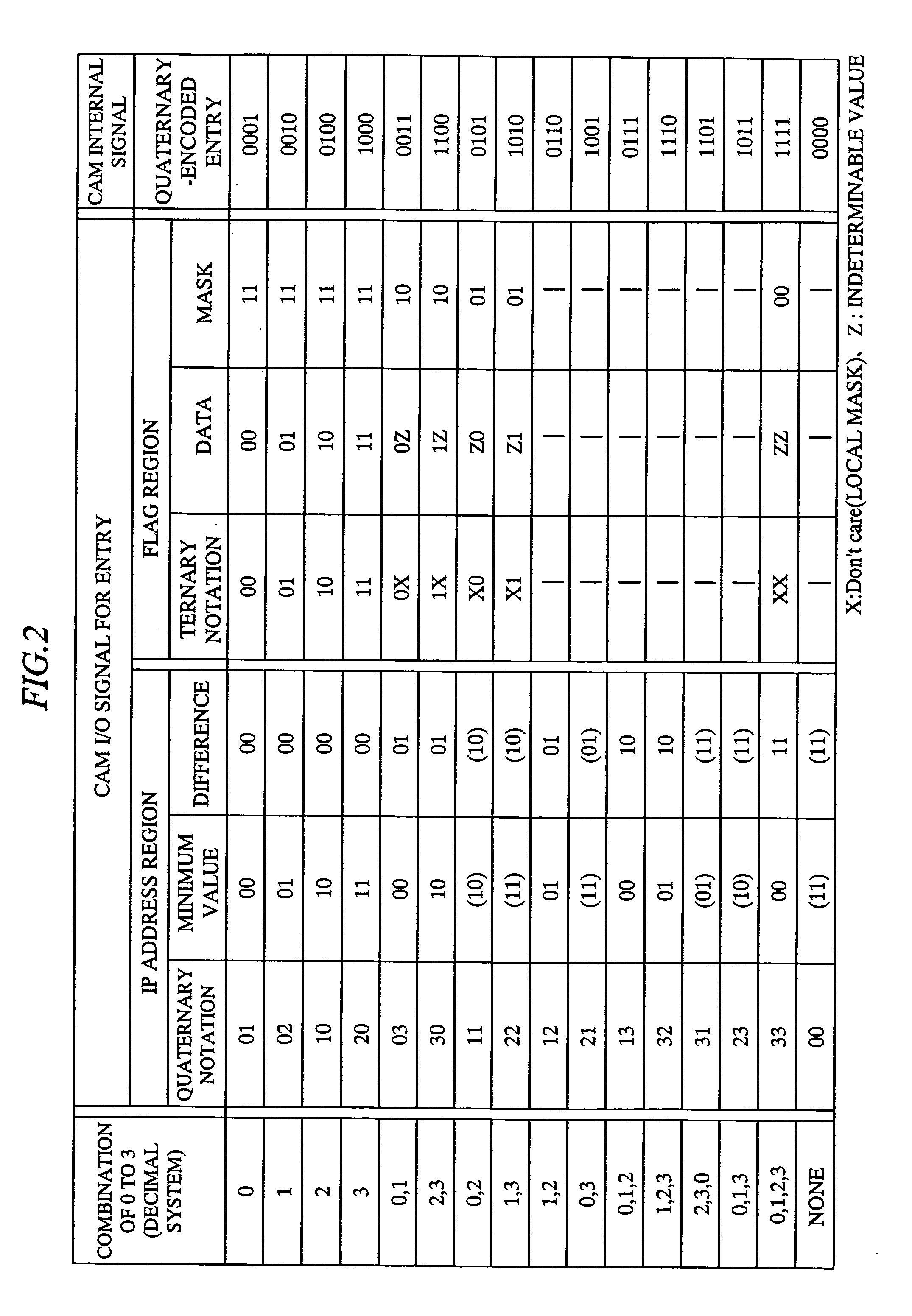
[0049]FIG. 2 shows an example of mapping of CAM I / O signal and One-hot-block code for the entry in the present invention with respect to the IP address region and the flag region, respectively. Although the detail will be described later, the I / O signals of this embodiment have the two features. The first feature is to use the binary information concerning the minimum value of each entry and the difference as the I / O signal in such an IP address region that a plurality of information is collectively stored. The second feature is that the data and the binary information concerning the mask are used as I / O signals similar to the conventional TCAM in the region as represented by the flag region whose range is never specified like the IP address.

[0050] First of all, I / O signals of the IP address region will be described. In FIG. 2, for the simplification, mapping of 2-bit I / O signals is shown for the case of 0-3 (decimal system) combinations. More concretely, the ...

second embodiment

[0146] Next, another example of the CAM operation using the One-hot-spot block code described in first embodiment will be described. The feature of this operation lies in the point that the operation time is shortened by making use of the wide bus width of the CAM data bus DQ and applying the address signal non-multiplexing system in which the low address X-ADD and the register address REG-ADD are simultaneously inputted. The write operation and the read operation thereof will be described as follows, respectively.

(Write Operation)

[0147]FIG. 15 shows the timing chart of write operation of CAM in this embodiment. FIG. 15 is based on the assumption similar to FIG. 6 and waveforms using the same symbols are shown.

[0148] First half of the first cycle (1A cycle): The command valid signal CMDV which is brought to the low level is driven to the high level and at the same time, the write command is inputted by using the command signal group CMD[1:0]. In addition, by setting the command ...

third embodiment

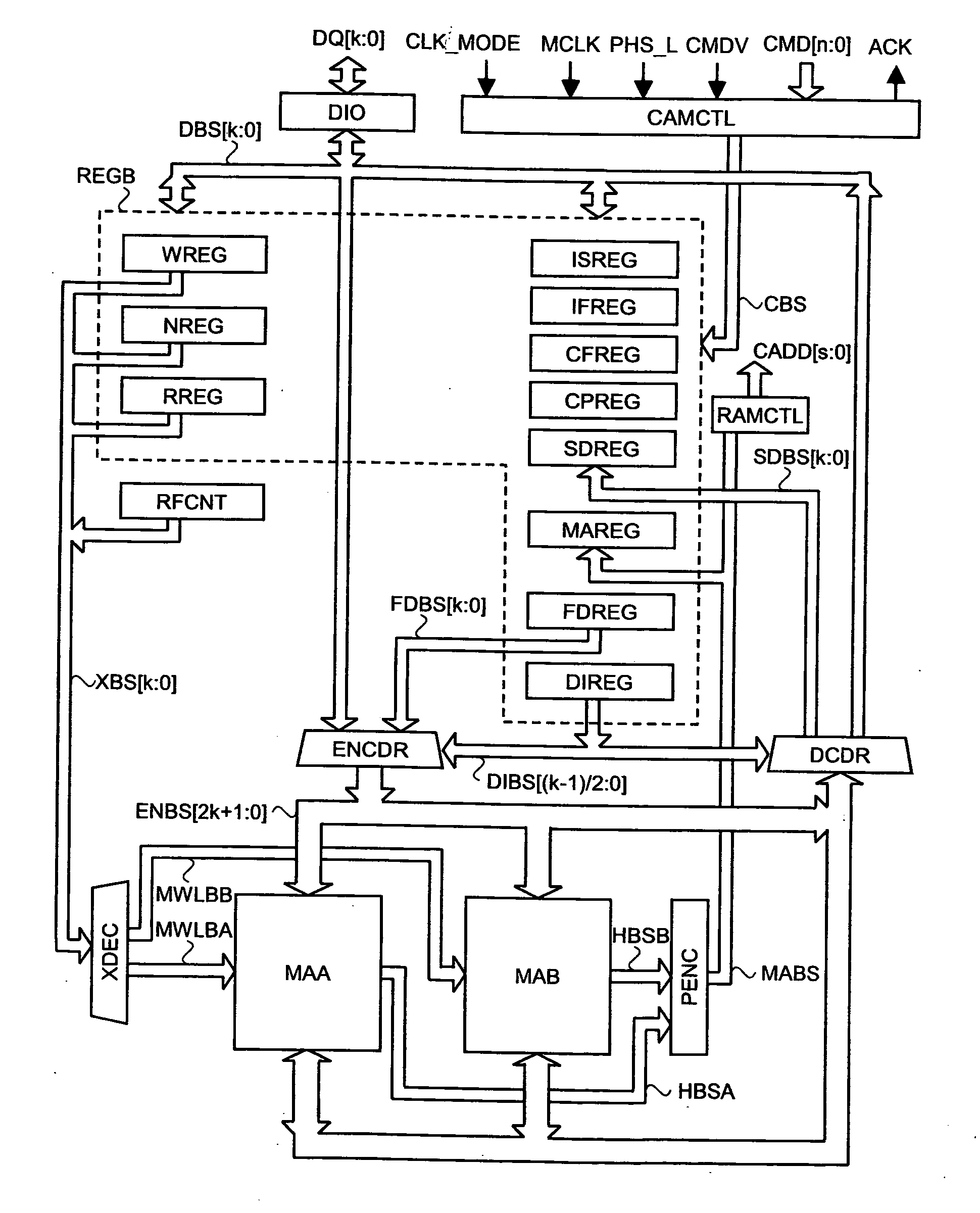
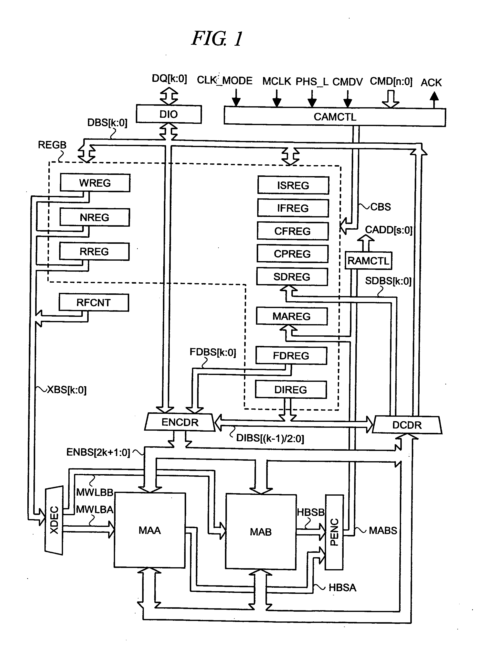
[0166] Next, another example of the floor plan of the CAM applying the One-hot-spot block code described in the first embodiment will be described with reference to FIG. 17. The feature of this configuration lies in the point that the interface circuit blocks IFB0 to IFB3 are arranged for each of the memory array blocks ARY0 to ARY3, and the entry and the search key are transmitted and received between the memory array blocks ARY0 to ARY3 via the corresponding encoding data buses ENBS0 to ENBS3. Here, similar to the interface circuit block IFB shown in FIG. 5, the interface circuit blocks IFB0 to IFB3 comprise the encoding circuit ENCDR, the decoding circuit DCDR, and the various register block REGB, respectively. Therefore, in the floor plan shown in FIG. 5, the interface circuit block IFB is arranged at the intersection regions of the cruciform regions. In the present embodiment, however, the interface circuit block IFB is arranged in the region in the transverse direction where t...


PUM


Abstract

In accordance with the regions which are component elements of memory information (entry) and input information (comparison information or search key), quaternary information including a pair of the minimum value and the difference or ternary information including a pair of the data and the mask are used as I/O signals. In addition, in accordance with the two types of information, two types of encoding circuits and decoding circuits are disposed, and either one of the encoding circuits and the decoding circuits are activated in accordance with the values set to the registers disposed to designate the format of information in each region of the entry and the search key. By selecting the desired register from the plurality of registers in response to the external command signals and address signals, the encoding and decoding in accordance with the information to be processed are carried out.

Description

CROSS-REFERENCE TO RELATED APPLICATION [0001] The present application claims priority from Japanese Patent Application JP 2004-169314 filed on Jun. 8, 2004, the content of which is hereby incorporated by reference into this application. TECHNICAL FIELD OF THE INVENTION [0002] The present invention relates to a semiconductor device. More specifically, it relates to a semiconductor device including a content addressable memory cell (CAM cell) which compares information stored in a storage node with inputted information and a semiconductor device including a CAM array which stores or compares information encoded in the device. BACKGROUND OF THE INVENTION [0003] As a result of explosive popularization of the Internet, the table scale required for a router and a switch in the network has been rapidly increasing, and the improvement of the search speed of the table has been demanded. For the achievement of this demand by means of hardware, ternary content addressable memory (TCAM) has att...

Claims


Application Information

Patent Timeline
IPC IPC(8): G11C15/00G11C15/04H04L45/74
CPCG11C15/00G11C15/043
Inventor HANZAWA, SATORUSEKIGUCHI, TOMONORITAKEMURA, RIICHIRO
Owner HITACHI LTD
Why Eureka
Try Eureka