

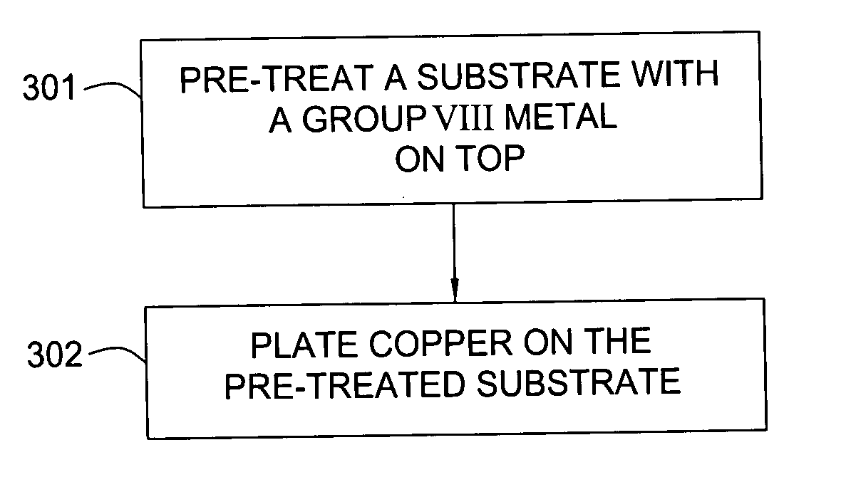
Plating chemistry and method of single-step electroplating of copper on a barrier metal
a technology of single-step electroplating and copper, which is applied in the direction of basic electric elements, electrical equipment, semiconductor devices, etc., can solve the problems of increasing the current density of such features, not consistently filling the structure of conventional deposition processes, and forming voids in the conductors
- Summary
- Abstract
- Description
- Claims
- Application Information
AI Technical Summary
Problems solved by technology
Method used
Image

Examples
example
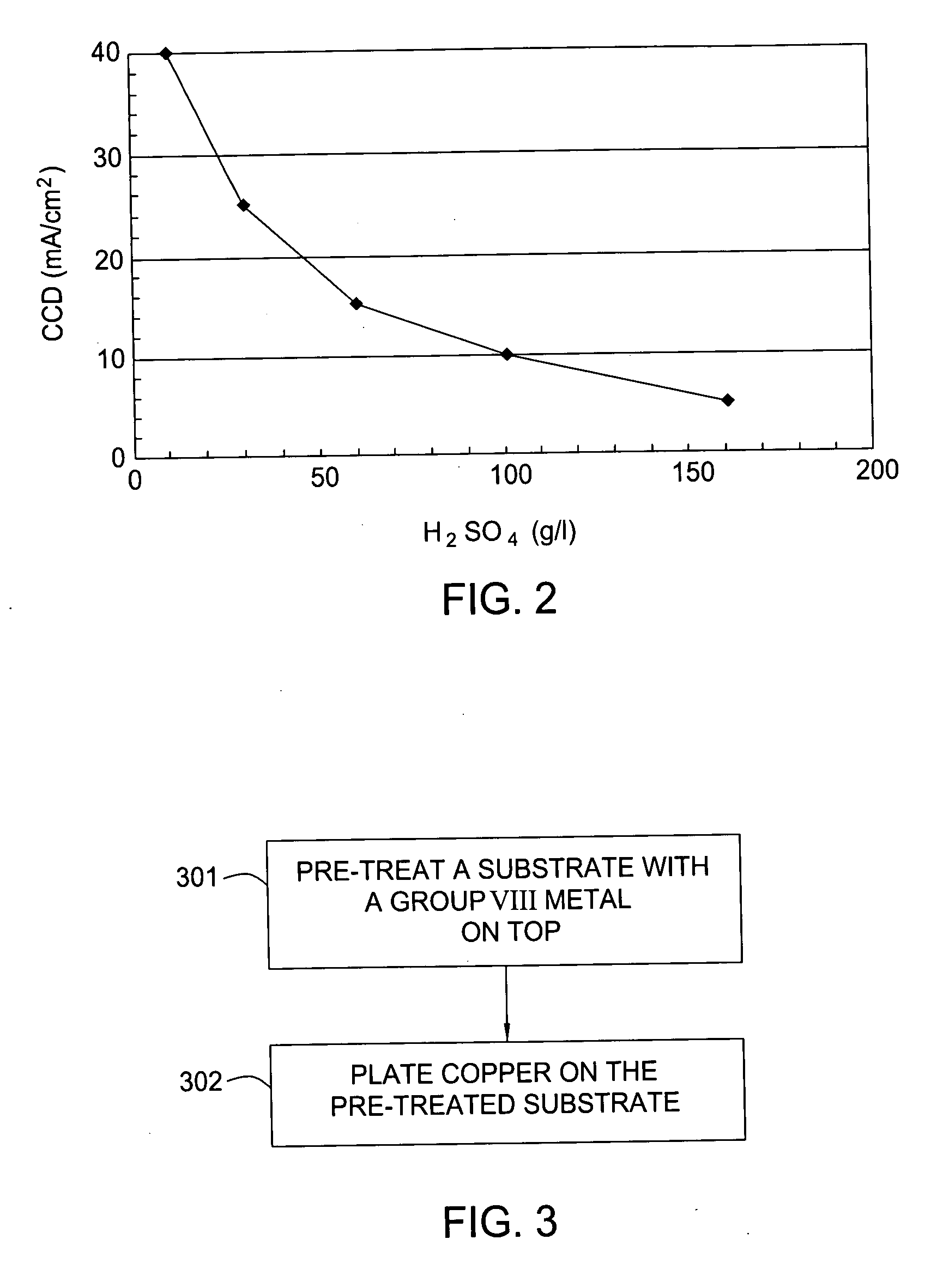
[0082]FIG. 10 shows the SEM of excellent gapfill of plated copper on an annealed Ru surface in 0.14 μm×0.8 μm trenches. The as-deposited Ru is an 80 Å ALD Ru. The pre-treatment process was performed on the substrate using a forming gas to anneal the wafer at temperature of 300° C. for 3 minutes. The plating solution used to gap-fill the features contained 40 g / l of copper, 100 g / l of sulfuric acid, 50 ppm of Cl ions, 12 ppm of sulfopropyl-disulfide (SPS) accelerator, 200 ppm of ethylene oxide and propylene oxide copolymers suppressor and 2 ml / l of ViaForm leveler. The plating bath was maintained at 18° C. The copper plating current was 10 mA / cm2 for the first 100 Å (for nucleation) and 5 mA / cm2 for the remaining 1900 Å deposition (for gap fill). Additional bulk-fill plating can be performed to reach the desired total thickness.
[0083] The experimental results and discussion related to Ru is merely used as examples. The inventive concept can be applied to other group VIII metals, suc...
PUM
| Property | Measurement | Unit |
|---|---|---|
| Temperature | aaaaa | aaaaa |
| Temperature | aaaaa | aaaaa |
| Temperature | aaaaa | aaaaa |
Abstract
Description
Claims
Application Information