Schottky barrier source/drain N-MOSFET using ytterbium silicide

a technology of ytterbium silicide and mosfet, which is applied in the direction of basic electric elements, electrical apparatus, and semiconductor devices, can solve the problems of large leakage currents in the device, poor film morphology of ersisub>2-x /sub>formed by solid-state reaction of as-deposited er and substrate si, and small drivability, so as to improve the electrical performance and reduce the barrier height. , the effect of improving

Inactive Publication Date: 2005-12-15
NAT UNIV OF SINGAPORE
View PDF13 Cites 19 Cited by
  • Summary
  • Abstract
  • Description
  • Claims
  • Application Information

AI Technical Summary

Benefits of technology

[0013] The invention can be used to fabricate Schottky barrier source / drain MOSFETs, especially when the device size is scaled down to sub-50 nm. Replacing ErSi2-x in N-SSDTs by YbSi2-x improves its electrical performance significantly with no accompanying disadvantages. It should, however, be noted that the present invention does not imply that other silicides, such as ternary silicides and germano-silicide may not yield similar improvements

Problems solved by technology

2 for example However, the drain current of a SSDT is suppressed by the Schottky barrier between source and channel, resulting in small drivability and low Ion / Ioff ratio.
However, the film morphology of ErSi2-x formed by solid-state reaction of as-deposited Er and substrate Si, is quite poor due to its island-preferred growth mode (see ref.
7), resulting in larger than theoretically expected leakage currents in the device.
Contacts prepared in conventional vacuum displayed larger barrier heights (0.37-0.39 eV) indicating that ultra high vacuum is necessary for ErSi2-x fabrication, which makes the process inconvenient and costly.

Method used


Image

  • Schottky barrier source/drain N-MOSFET using ytterbium silicide
  • Schottky barrier source/drain N-MOSFET using ytterbium silicide
  • Schottky barrier source/drain N-MOSFET using ytterbium silicide

Examples


Embodiment Construction

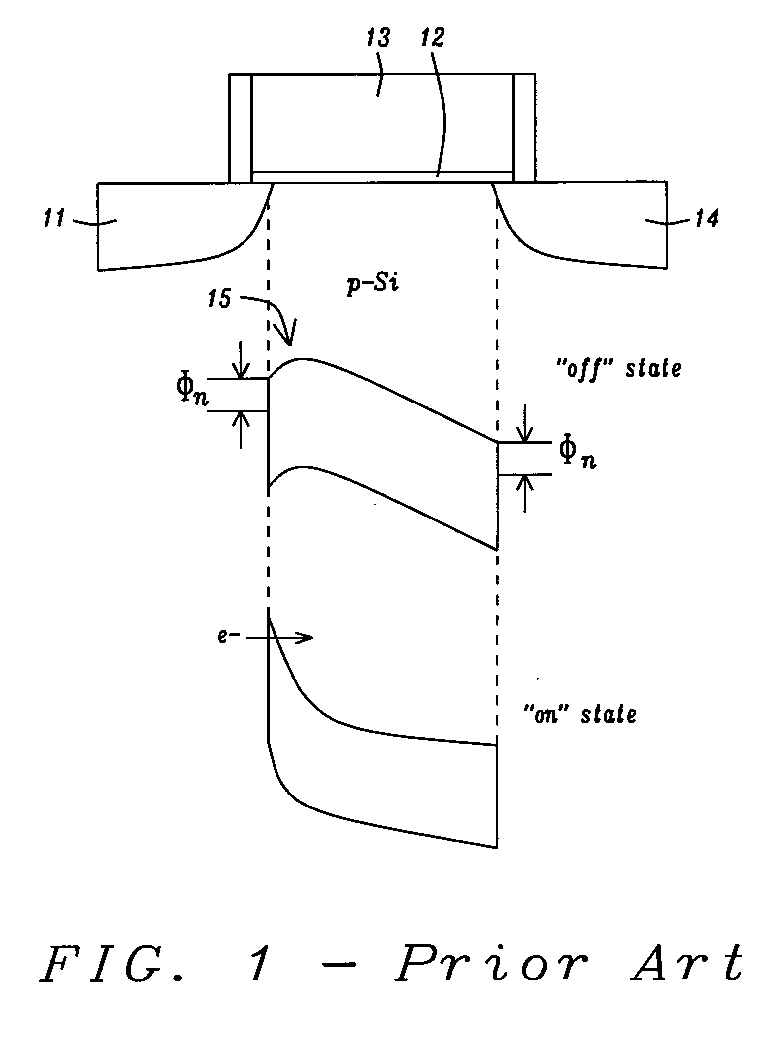
[0022] In this invention a N-SSDT device having YbSi2-x, source and drain is disclosed. The schematic structure and operating principles are illustrated in FIG. 1. Seen there are source 11, gate oxide 12, gate electrode 13, and drain 14. In the off state, barrier 15 slopes away from the P silicon-source interface and current flow is blocked. In the on state, the barrier is still present but has grown thin enough for current to pass through it through Fowler-Nordheim tunneling.

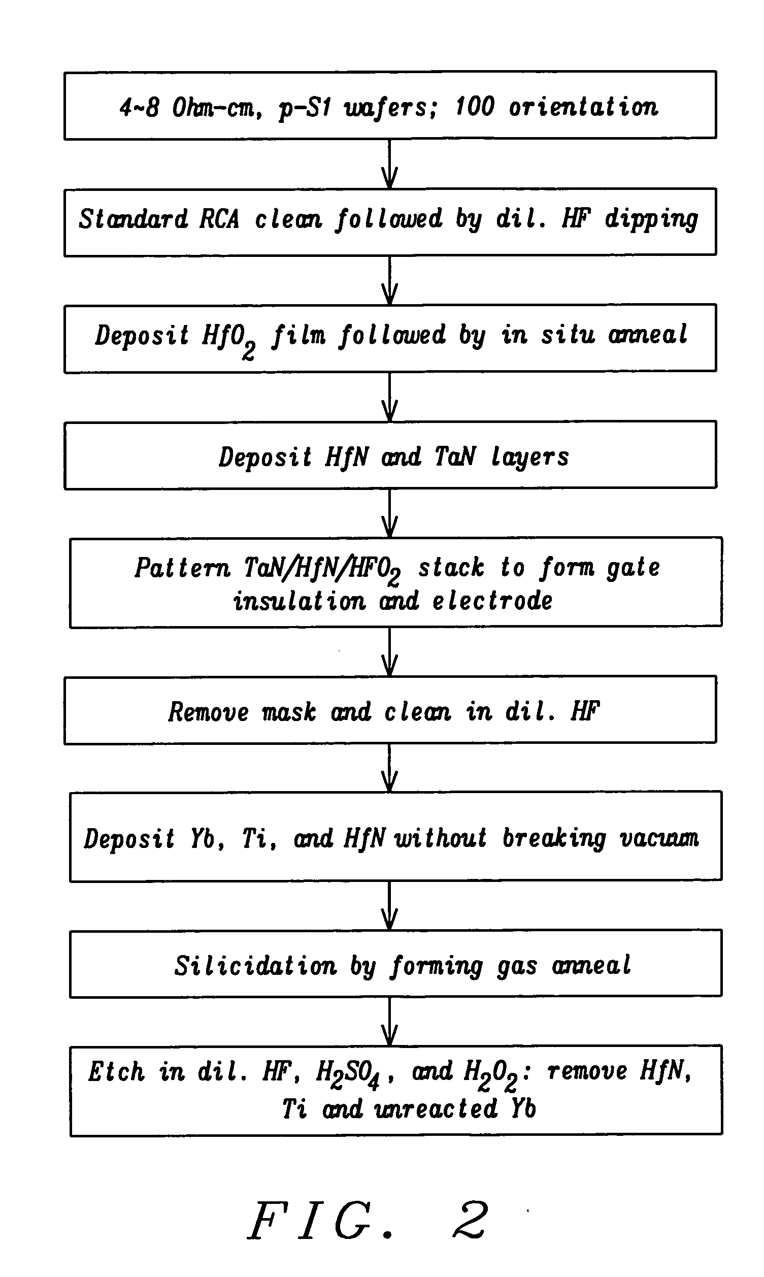
[0023] To avoid the introduction of unnecessary detail, a simple single mask process, which has been demonstrated in our lab, is described here. The performance of the resulting device has been compared with that of an ErSi2-x S / D device fabricated by the same method. It will be understood that the basic principles of the invention will continue to apply to more detailed versions of this simplified process.

[0024] It is also important to note that the self-aligned YbSi2-x process described here is fully compat...


PUM


Abstract

A method of fabricating an N-type Schottky barrier Source / Drain Transistor (N-SSDT) with ytterbium silicide (YbSi2-x) for source and drain is presented. The fabrication of YbSi2-x is compatible with the normal CMOS process but ultra-high vacuum, which is required for ErSi2-x fabrication, is not needed here. To prevent oxidation of ytterbium during ex situ annealing and to improve the film quality, a suitable capping layer stack has been developed.

Description

[0001] This application claims priority to U.S. Provisional Patent Application Ser. No. 60 / 470,126, filed on May 11, 2004, which is herein incorporated by reference in its entirety.FIELD OF THE INVENTION [0002] The invention relates to nanoscale MOSFET architecture, in particular to an improved high performance N-type Schottky barrier source / drain MOSFET. BACKGROUND OF THE INVENTION [0003] SSDTs (Schottky barrier Source / Drain Transistors), where the highly doped source / drain of the conventional MOSFET is totally replaced with a silicide, were first reported by M. P. Lepselter and S. Sze in 1968 (see ref. 1). Recently, SSDTs have received a great deal of attention due to their excellent scaling properties and ease of fabrication and have been proposed as an alternative to traditional MOSFETs for sub-100 nm integration. See ref. 2 for example However, the drain current of a SSDT is suppressed by the Schottky barrier between source and channel, resulting in small drivability and low Io...

Claims


Application Information

Patent Timeline
Patent Type & Authority Applications(United States)
IPC IPC(8): H01L21/28H01L21/285H01L21/336H01L29/47H01L29/49H01L29/51H01L29/76H01L29/78
CPCH01L21/28088H01L21/28185H01L21/28518H01L29/47H01L29/4966H01L29/517H01L29/66643H01L29/7839
Inventor ZHU, SHIYANGCHEN, JINGDELEE, SUNG JOOLI, MING FUSINGH, JAGARZHU, CHUNXIANGKWONG, DIM-LEE
Owner NAT UNIV OF SINGAPORE
Why Eureka
Try Eureka