Voltage controlled oscillator, and PLL circuit and wireless communication apparatus using the same

a technology of voltage control and oscillator, which is applied in the direction of oscillator, pulse automatic control, pulse technique, etc., can solve the problems of decrease in frequency tuning sensitivity, and difficulty in obtaining substantially the same frequency tuning sensitivity over the wide variable-frequency range, etc., to achieve the effect of suppressing the deterioration of phase noise characteristics

Active Publication Date: 2005-12-15
PANASONIC CORP
View PDF1 Cites 18 Cited by
  • Summary
  • Abstract
  • Description
  • Claims
  • Application Information

AI Technical Summary

Benefits of technology

[0026] Therefore, an object of the present invention is to provide a voltage controlled oscillator which can suppress a deterioration in phase noise characteristics and control a range of variable frequency over a wide band to obtain substantially the same frequency tuning sensitivity over the variable-frequency range, and a PLL circuit and a wireless communication apparatus using the same.

Problems solved by technology

However, it is difficult to obtain substantially the same frequency tuning sensitivity over the entire wide variable-frequency range.
As the oscillation frequency is lowered, a ratio of the capacitance change amount of the variable capacitance circuit to the total capacitance value of the resonant circuit is decreased, resulting in a decrease in the frequency tuning sensitivity.
However, in the conventional improved method of FIG. 15, the switching elements 553, 554, 563, 564, 573, 574 are provided in portions of the variable capacitance circuits 550, 560, 570 through which a high-frequency signal flows, and therefore, phase noise characteristics are deteriorated due to loss in the switching elements.
For example, when the switching element is a MOS switch, loss occurs in the on-resistance, resulting in a deterioration in the phase noise characteristics.

Method used


Image

  • Voltage controlled oscillator, and PLL circuit and wireless communication apparatus using the same
  • Voltage controlled oscillator, and PLL circuit and wireless communication apparatus using the same
  • Voltage controlled oscillator, and PLL circuit and wireless communication apparatus using the same

Examples


first embodiment

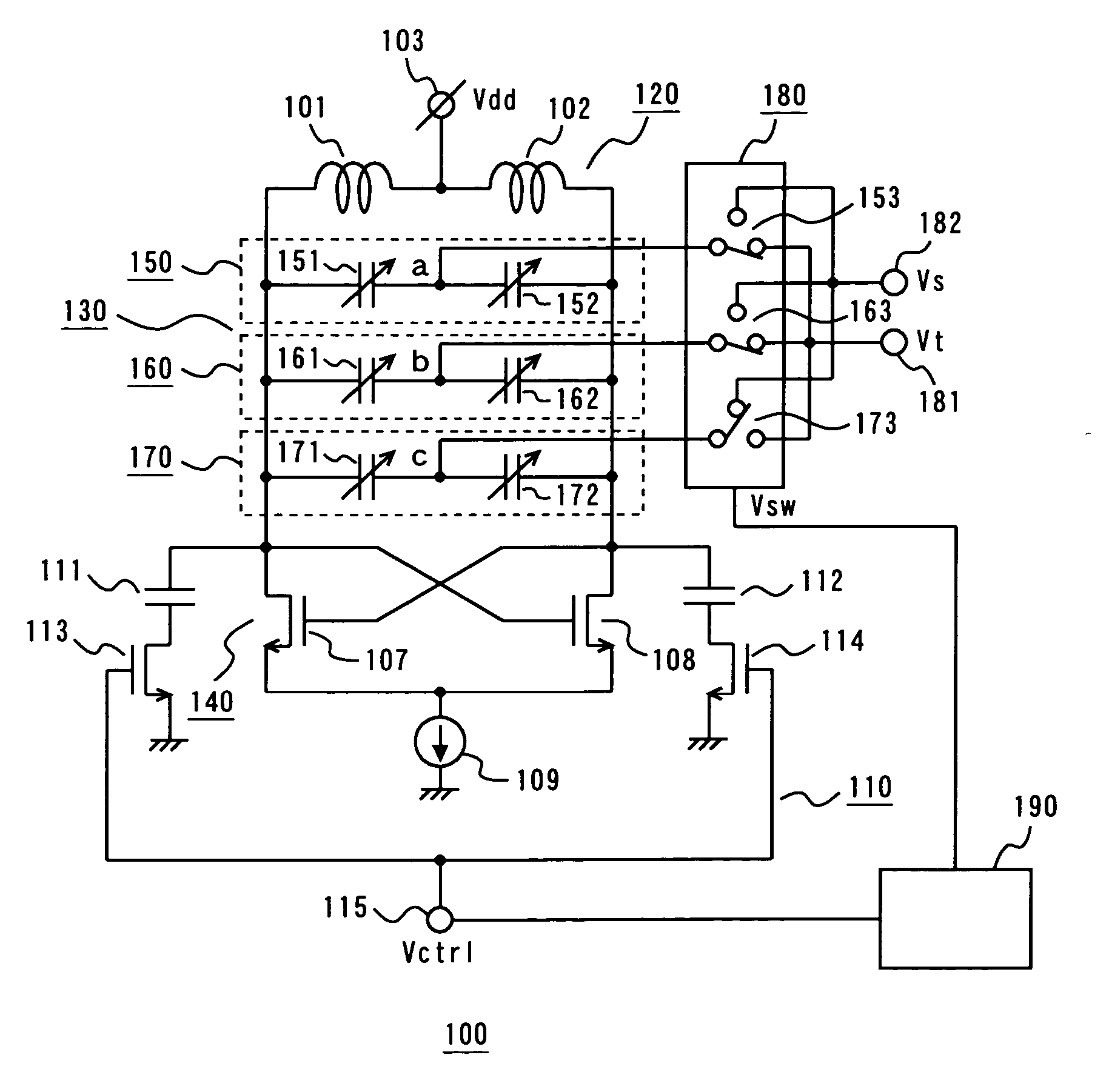
[0092]FIG. 1 is a circuit diagram illustrating a voltage controlled oscillator 100 according to a first embodiment of the present invention. Note that a bias circuit and the like are not illustrated in FIG. 1.

[0093] In FIG. 1, the voltage controlled oscillator 100 comprises an inductor circuit 120, a negative resistance circuit 140, a high-frequency switch circuit (band switching circuit) 110, a first variable capacitance circuit 150 (hereinafter referred to as a variable capacitance circuit A), a second variable capacitance circuit 160 (hereinafter referred to as a variable capacitance circuit B), a third variable capacitance circuit 170 (hereinafter referred to as a variable capacitance circuit C), a frequency tuning sensitivity control section 180, and a frequency control section 190. The inductor circuit 120, the negative resistance circuit 140, the high-frequency switch circuit 110, the variable capacitance circuit A, the variable capacitance circuit B, and the variable capaci...

second embodiment

[0142]FIG. 6A is a block diagram illustrating a structure of a PLL circuit according to a second embodiment of the present invention. The above-described voltage controlled oscillator of the first embodiment is mainly used in PLL circuits, such as that illustrated in FIG. 6A. In FIG. 6A, a PLL circuit 300 comprises a phase comparator 301, a loop filter 302, a voltage controlled oscillator 303, and a frequency divider 304. The PLL circuit is a circuit which fixes (locks) an oscillation frequency to a desired frequency. The voltage controlled oscillator 303 is similar to the voltage controlled oscillator of the first embodiment. The phase comparator 301 compares a phase of an input reference signal with a phase of a signal obtained by frequency-dividing an output signal of the voltage controlled oscillator 303 using the frequency divider 304. An output signal of the phase comparator 301 is input to the loop filter 302. The loop filter 302 converts the output signal of the phase compar...

third embodiment

[0153]FIG. 8 is a circuit diagram illustrating a structure of a variable capacitance circuit used in a voltage controlled oscillator according to a third embodiment of the present invention. The variable capacitance circuit 200 of FIG. 8 is used as the variable capacitance circuit 130 of the voltage controlled oscillator 100 of FIG. 1.

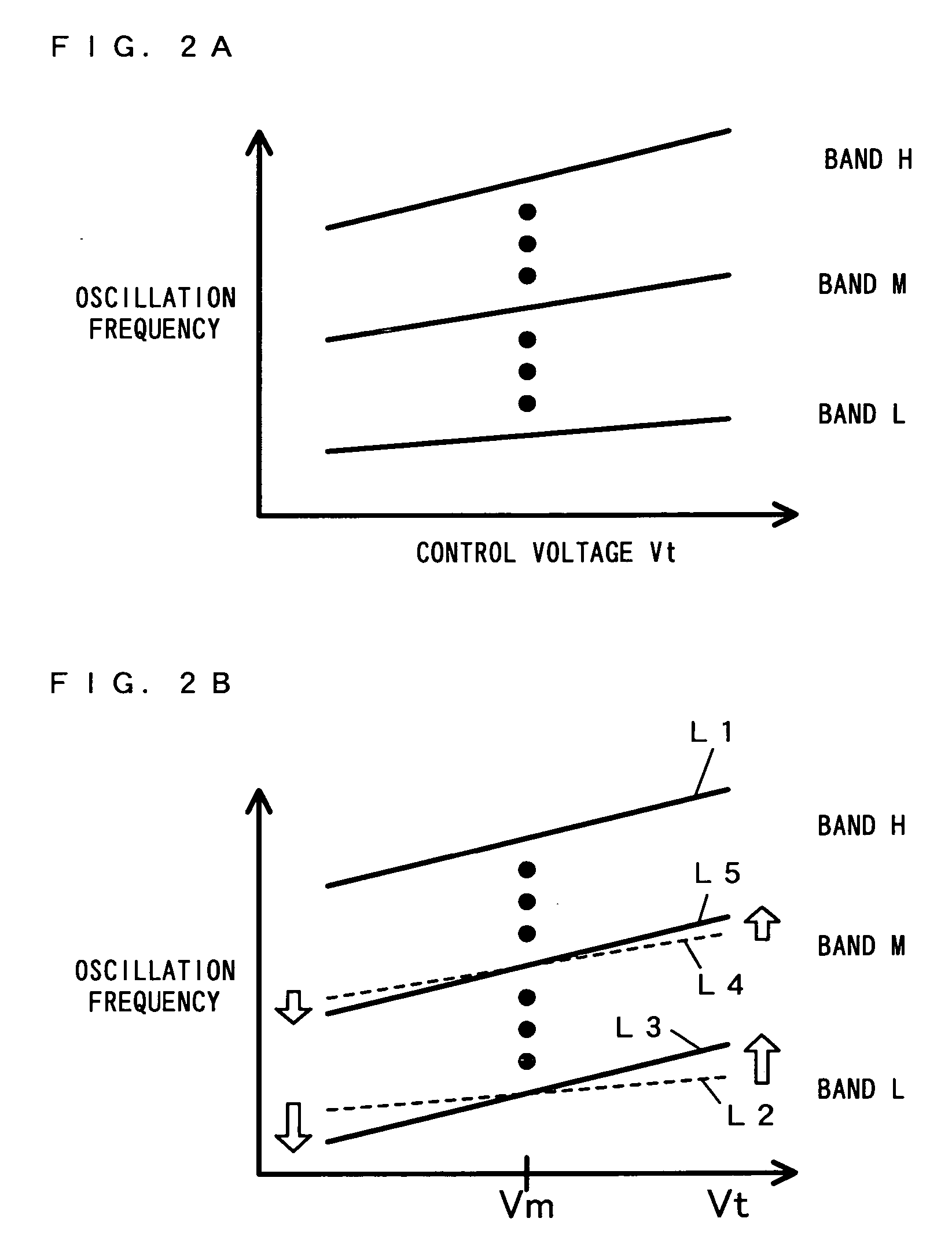
[0154] The frequency tuning sensitivity of a voltage controlled oscillator is substantially determined based on characteristics of a variable capacitance element used therein. Therefore, the variable capacitance element preferably has characteristics such that a capacitance thereof is moderately changed over a wide control voltage range. Actually, when the voltage controlled oscillator is implemented on a semiconductor substrate, it is difficult to use a variable capacitance element having a high level of linearity.

[0155] In the voltage controlled oscillator of the first embodiment, the frequency tuning sensitivity is approximated as being linear. Ho...


PUM


Abstract

A voltage controlled oscillator comprises a parallel resonance circuit including an inductor circuit, a variable capacitance circuit, and a high-frequency switch circuit, a negative resistance circuit and a frequency control section, and a frequency tuning sensitivity control section. The frequency control section shifts a band of an oscillation frequency by controlling ON/OFF of a switching element included in the high-frequency switch circuit. The frequency tuning sensitivity control section adjusts a change rate of a total capacitance of the variable capacitance circuit with respect to a control voltage, depending on a band to be used. The frequency tuning sensitivity control section is connected to a virtual ground point of a differential signal.

Description

BACKGROUND OF THE INVENTION [0001] 1. Field of the Invention [0002] The present invention relates to a voltage controlled oscillator, and a PLL circuit and a wireless communication apparatus which employ the same. More particularly, the present invention relates to a voltage controlled oscillator having a band switching function, and a PLL circuit and a wireless communication apparatus which employ the same. [0003] 2. Description of the Background Art [0004] Voltage control oscillators are widely used as means for generating a local oscillation signal for wireless communication apparatuses. The voltage controlled oscillator, when manufactured as a high-frequency IC, requires a wide oscillation frequency range to tolerate variations in the components caused by the semiconductor manufacturing process. Recently, there is a demand for a voltage controlled oscillator which has an oscillation frequency variable over a wide frequency range in order to support a communication system which e...

Claims


Application Information

Patent Timeline
Patent Type & Authority Applications(United States)
IPC IPC(8): H03B5/00H03B5/08H03B5/12
CPCH03B2200/0048H03B2200/0098H03L7/099H03L7/18H03B5/1228H03B5/1215H03B5/1265H03B5/1293
Inventor TSUKIZAWA, TAKAYUKITAKINAMI, KOJIOHARA, ATSUSHIADACHI, HISASHI
Owner PANASONIC CORP
Why Eureka
Try Eureka