Semiconductor electro-absorption optical modulator, semiconductor electro-absorption optical modulator integrated laser, optical transmitter module and optical module

Active Publication Date: 2005-12-15
LUMENTUM JAPAN INC
View PDF6 Cites 15 Cited by
  • Summary
  • Abstract
  • Description
  • Claims
  • Application Information

AI Technical Summary

Benefits of technology

[0012] That is, by increasing the length of the EA modulator, the ACER equivalent to that at high temperature can be obtained at low temperature. In this invention, by providing a plurality of electrodes onto the EA modulator, the ACER which is obtained when a signal voltage is applied to only one electrode at high temperature can be obtained even at low temperature. More specifically, since the signal voltage is applied also to other electrodes in a low-temperature operation, the effective operation

Problems solved by technology

When the detune amount is large, even if a voltage applied is increased, the EA modulator cannot sufficiently absorb light.
However, when the temperature control mechanism is not ne

Method used


Image

  • Semiconductor electro-absorption optical modulator, semiconductor electro-absorption optical modulator integrated laser, optical transmitter module and optical module
  • Semiconductor electro-absorption optical modulator, semiconductor electro-absorption optical modulator integrated laser, optical transmitter module and optical module
  • Semiconductor electro-absorption optical modulator, semiconductor electro-absorption optical modulator integrated laser, optical transmitter module and optical module

Examples


first embodiment

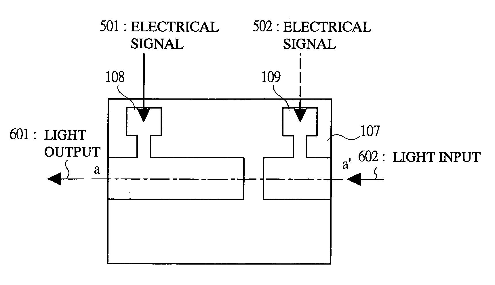
[0025] A first embodiment of the present invention is characterized by the followings. That is, an EA modulator is provided, in which an optical waveguide formed of a multi-layer film is formed on a substrate, an electrical signal is applied to the optical waveguide in a direction vertical to the substrate, and the absorption amount of inputted light is changed so as to control the amount of light to be outputted. Also, a plurality of electrodes which are electrically separated from each other are arranged in the EA modulator, and when an electrical signal is applied to the EA modulator, the number of electrodes to which the signal is applied differs depending on temperature.

[0026] With reference to FIGS. 1A and 1B, an example of the configuration of the EA modulator according to the first embodiment will be described. FIG. 1A is a plan view illustrating the EA modulator, and FIG. 1B is a sectional view taken along the line a-a′ in FIG. 1A.

[0027] The EA modulator of this embodimen...

second embodiment

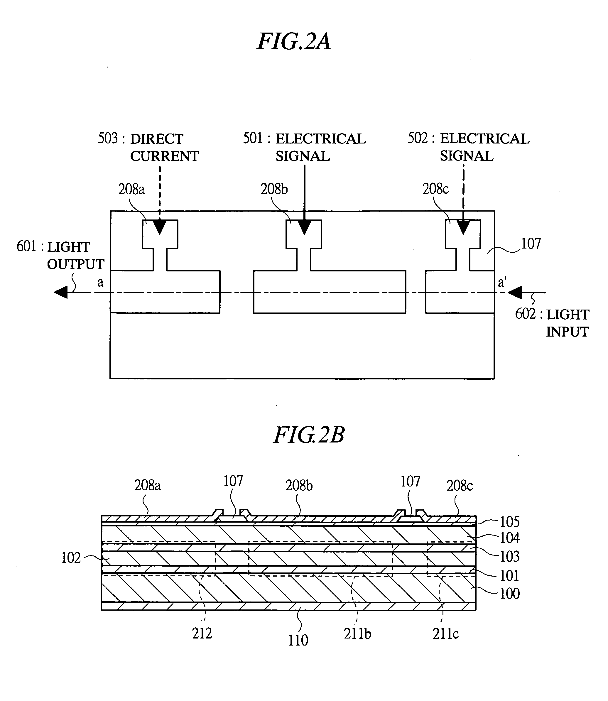
[0038] A second embodiment of the present invention is characterized by the followings. That is, a plurality of electrodes which are electrically separated from each other are arranged in the EA modulator described in the first embodiment, and when an electrical signal is applied to the EA modulator, the number of electrodes to which the electrical signal is applied differs depending on the temperature. In addition, a direct current in a forward direction is injected into electrodes to which the electrical signal is not applied. More specifically, the second embodiment is an example in which the direct current is injected into the electrodes to which an electrical signal is not applied at the time of the high-temperature operation.

[0039] With reference to FIGS. 2A and 2B, one example of the configuration of the EA modulator according to the second embodiment will be described. FIG. 2A is a plan view of the EA modulator, and FIG. 2B is a sectional view taken along the line a-a′ in F...

third embodiment

[0049] A third embodiment of the present invention is applied to an EA modulator integrated DFB laser, in which the EA modulator described in the first and second embodiments and the semiconductor laser device are integrated on one chip in a monolithic manner.

[0050] With reference to FIGS. 3A and 3B, one example of a configuration of the EA modulator integrated DFB laser according to the third embodiment will be described. FIG. 3A is a plan view of the EA modulator integrated DFB laser, and FIG. 3B is a sectional view taken along the line a-a′ in FIG. 3A.

[0051] The EA modulator integrated DFB laser according to the third embodiment is an example of a semiconductor EA modulator integrated DFB laser with wavelength of 1.5 μm band for optical transmission of 40 km at transmission rate of 10 Gbit / s. This device is formed in the manner as follows. First, after an oxide film mask for selective growth is formed on the n-type InP semiconductor substrate 100, as the first crystal growth, t...


PUM


Abstract

This invention provides an optical transmitter module and an optical module using an EA modulator capable of realizing stable ACER regardless of operating temperature without using a control mechanism for maintaining temperature of the EA modulator constant. In the EA modulator, optical waveguides formed of a multi-layered film are formed on a substrate, an electrical signal is applied to the optical waveguides in a direction vertical to the substrate, and the input light absorption amount is changed to control the amount of output light. Also, a plurality of p-side electrodes electrically separated from each other for applying an electrical signal to the active layer optical waveguides are arranged on optical axes of active layer optical waveguides. The length of optical waveguides to which the electrical signal is applied is changed by controlling the number of p-side electrodes to which the electrical signal is applied in accordance with temperature.

Description

CROSS-REFERENCE TO RELATED APPLICATION [0001] The present application claims priority from Japanese Patent Application JP 2004-173450 filed on Jun. 11, 2004, the content of which is hereby incorporated by reference into this application. TECHNICAL FIELD OF THE INVENTION [0002] The invention relates to a semiconductor electro-absorption optical modulator (hereinafter, referred to as EA (Electro-Absorption) modulator) having a plurality of electrodes. More particularly, it relates to a technique which is effective when applied to a semiconductor EA optical modulator integrated laser, in which the EA modulator and a semiconductor laser device are integrated, an optical transmitter module, and an optical module. BACKGROUND OF THE INVENTION [0003] Conventionally, the EA modulator used in an optical communication system is used in combination with a semiconductor laser device as an optical transmitter module, and generally has the configuration as follows. That is, in this configuration, ...

Claims


Application Information

Patent Timeline
IPC IPC(8): G02F1/017G02F1/03G02F1/07H01S5/022H01S5/026
CPCB82Y20/00G02F2203/21G02F1/01708
Inventor SUMI, SEIJIUOMI, KAZUHISAKAMIYAMA, HIROYUKINAOE, KAZUHIKO
Owner LUMENTUM JAPAN INC
Why Eureka
Try Eureka