

Method of embedding semiconductor element in carrier and embedded structure thereof
- Summary
- Abstract
- Description
- Claims
- Application Information
AI Technical Summary
Benefits of technology
Problems solved by technology
Method used
Image

Examples
first preferred embodiment
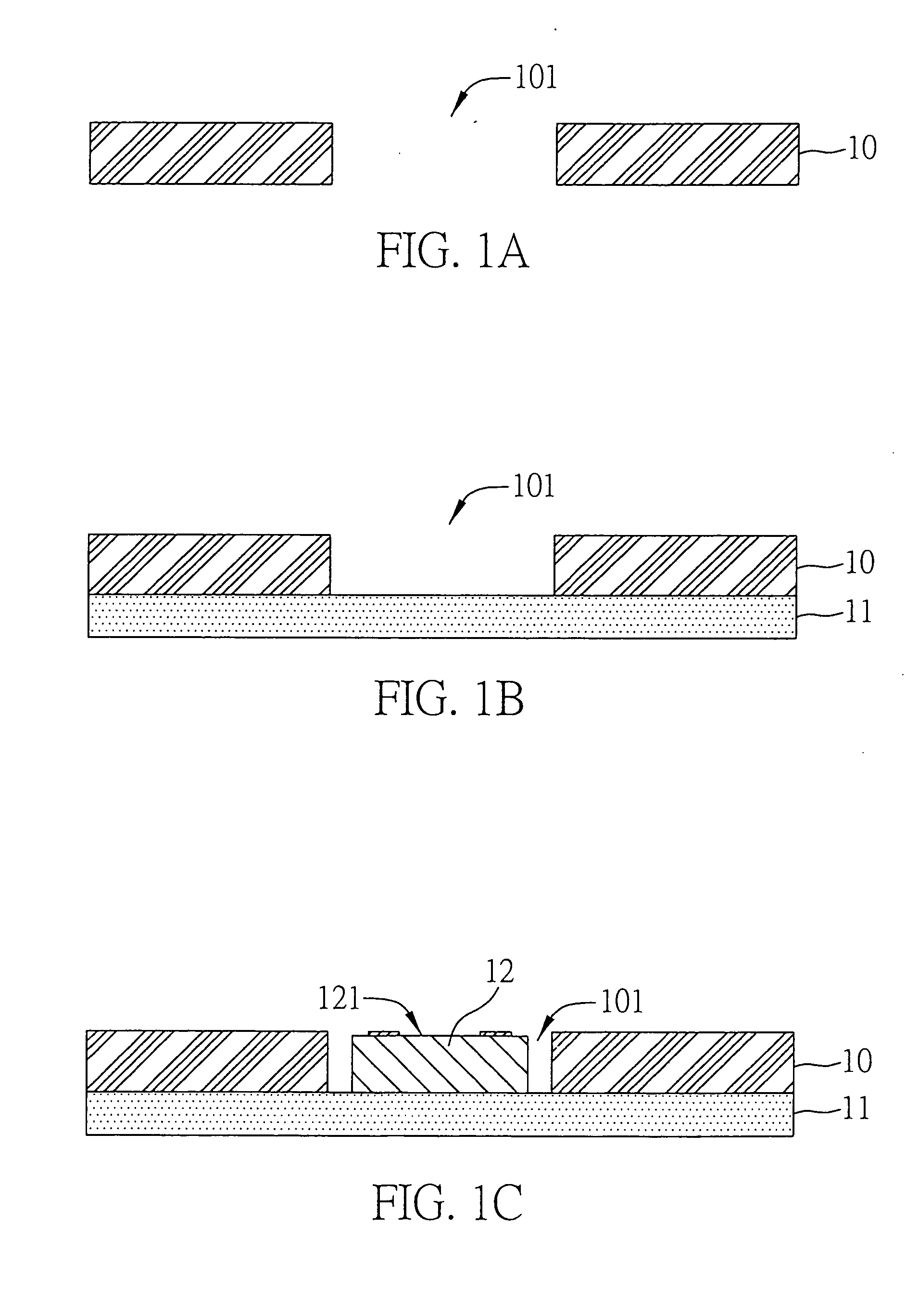
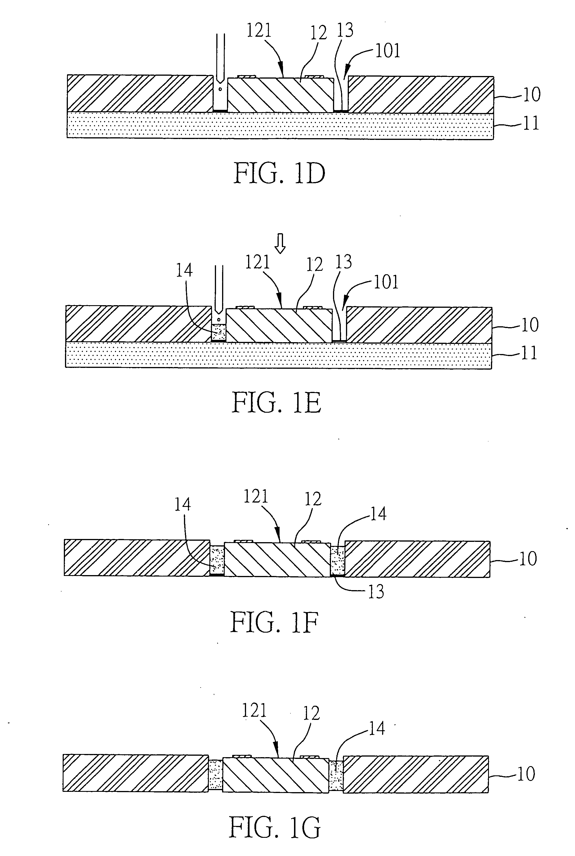
[0032]FIGS. 1A to 1G show procedural steps of a method of embedding a semiconductor element in a carrier in accordance with a first preferred embodiment of the present invention.
[0033] Referring to FIG. 1A, first, a carrier 10 is prepared, which can be an insulating board, metal board, or circuit board having a circuit layer. At least one hole 101 is formed through the carrier 10.
[0034] Referring to FIG. 1B, an auxiliary material 11 is attached to the bottom of the carrier 10 and temporarily seals a bottom opening of the hole 101 of the carrier 10. The auxiliary material 11 can be made as a film, dry film, insulating board or metal board, and a surface of the auxiliary material 11 in contact with the carrier 10 can be made adhesive or slightly adhesive.
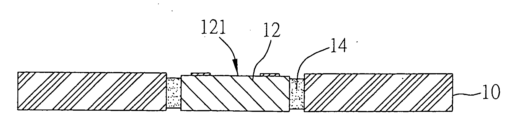
[0035] Referring to FIG. 1C, a semiconductor element 12 such as semiconductor chip is placed in the hole 101 of the carrier 10 in a manner that an active surface 121 of the semiconductor element 12 is exposed from the hole 101 and ...
second preferred embodiment
[0040]FIGS. 2A to 2G show procedural steps of the method of embedding a semiconductor element in a carrier in accordance with a second preferred embodiment of the present invention. In this embodiment, an auxiliary material used is the same as that of the first embodiment with its surface being made adhesive, slightly adhesive or non-adhesive.
[0041] Referring to FIGS. 2A and 2B, first, a carrier 10 having a hole 101 is provided. A slightly adhesive auxiliary material 11 is attached to the bottom surface of the carrier 10 and temporarily seals a bottom opening of the hole 101 of the carrier 10.
[0042] Referring to FIG. 2C, a medium material 13 is applied in the hole 101 to form a layer of medium material 13 at the bottom of the hole 101.
[0043] Referring to FIG. 2D, then a semiconductor element 12 is place in the hole 101 in a manner that an active surface 121 of the semiconductor element 12 is exposed from the hole 101. Since the medium material 13 when in a liquid phase before bei...
PUM
 Abstract
Description
Claims
Application Information