

Methods of forming semiconductor constructions
a technology of semiconductor construction and semiconductor structure, which is applied in the direction of semiconductor devices, semiconductor/solid-state device details, electrical devices, etc., can solve the problems of poor performance characteristics of dies, unacceptably high rejection rate of dies, and wrong curvature of dies
- Summary
- Abstract
- Description
- Claims
- Application Information
AI Technical Summary
Benefits of technology
Problems solved by technology
Method used
Image

Examples
Embodiment Construction
[0021] This disclosure of the invention is submitted in furtherance of the constitutional purposes of the U.S. Patent Laws “to promote the progress of science and useful arts” (Article 1, Section 8).
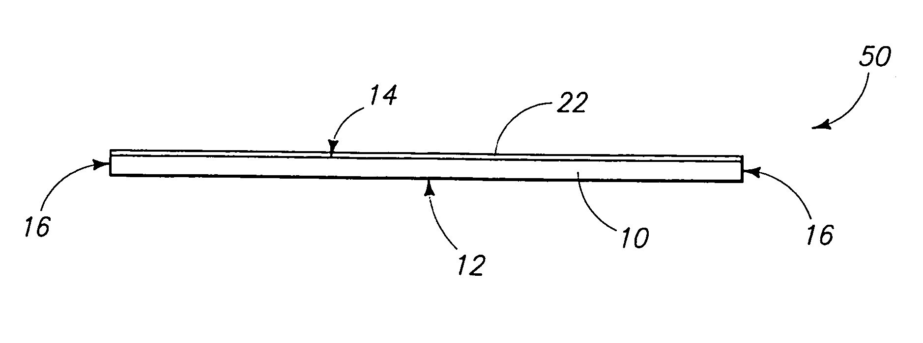
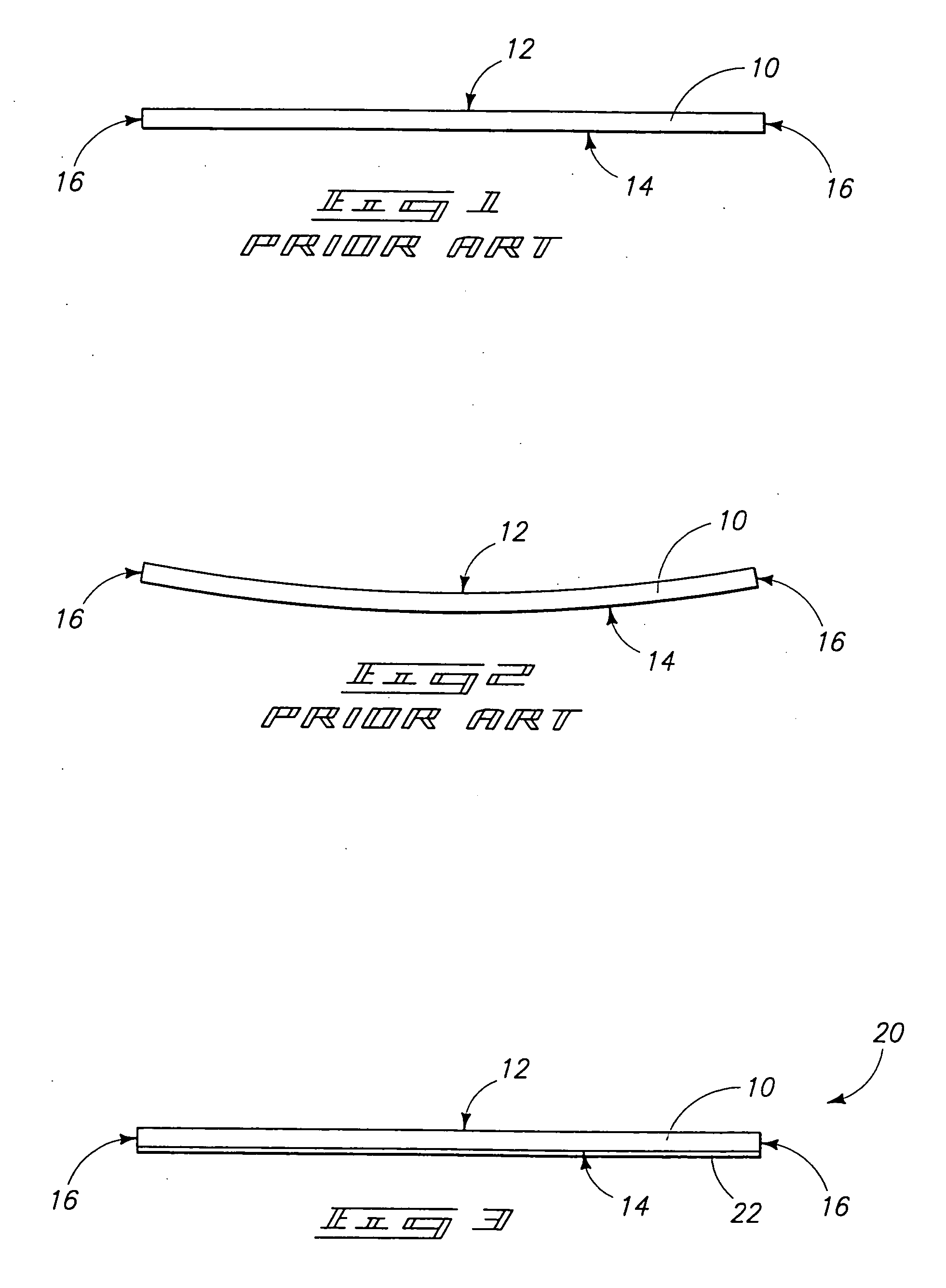
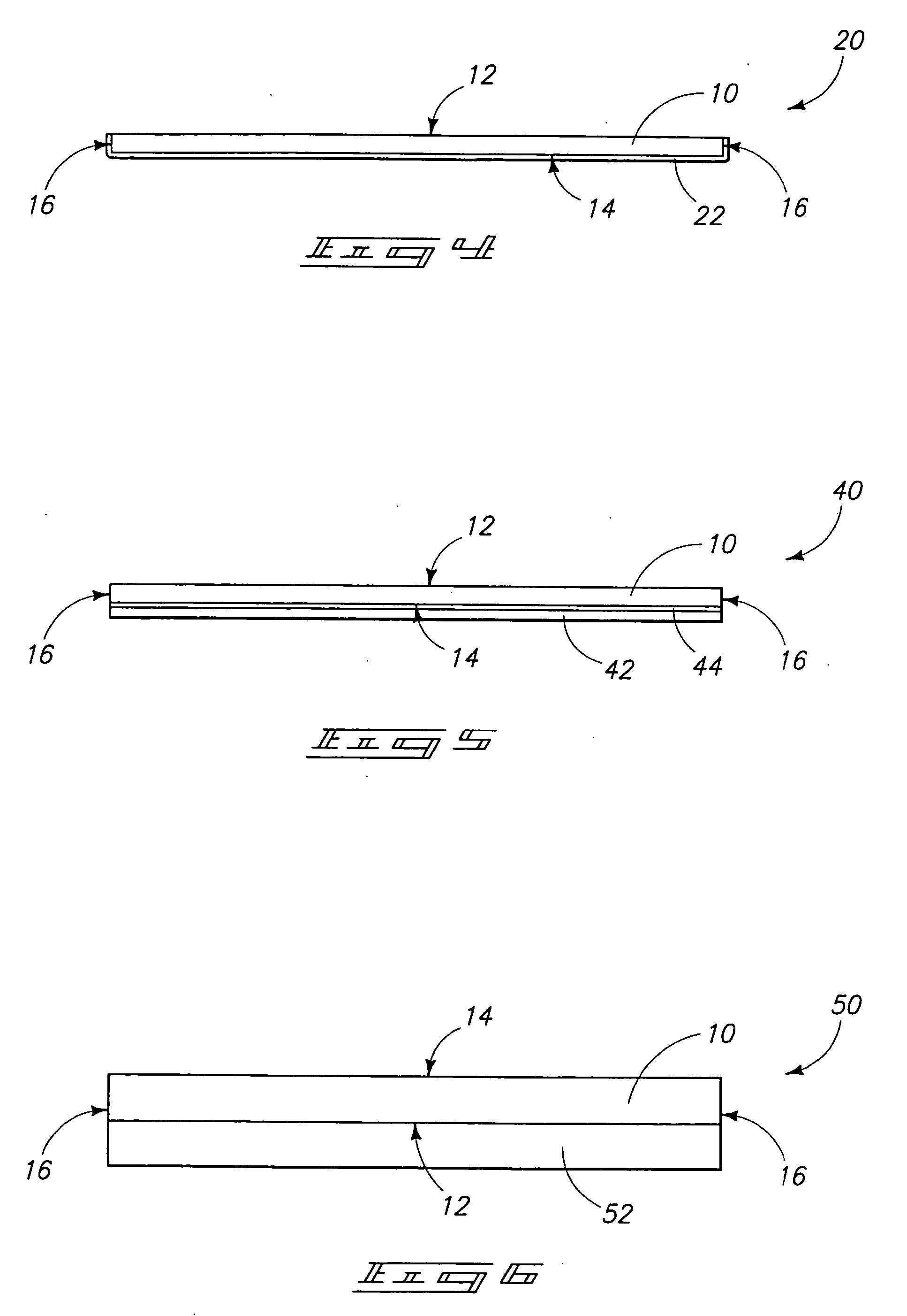
[0022] One aspect of the present invention is a recognition that the failure of semiconductor constructions comprising thin semiconductor material dies may be caused, at least in part, by ions diffusing interstitially or substitutionally to junction regions and recombining to reduce the minority carrier lifetime. Various ions may be formed during semiconductor processing, including, for example, metallic ions. One approach to reducing damage caused by such ions is to reduce or eliminate the ions during fabrication of semiconductor materials. Accordingly, efforts can be made to complete the fabrication in ultra-clean environments. However, it is difficult in practice to completely eliminate ions from entering at least some semiconductor constructions during a fabrication process. Another...
PUM
| Property | Measurement | Unit |
|---|---|---|
| Temperature | aaaaa | aaaaa |
| Temperature | aaaaa | aaaaa |
| Temperature | aaaaa | aaaaa |
Abstract
Description
Claims
Application Information