Data recording apparatus
- Summary
- Abstract
- Description
- Claims
- Application Information
AI Technical Summary
Benefits of technology
Problems solved by technology
Method used
Image
Examples
embodiment 1
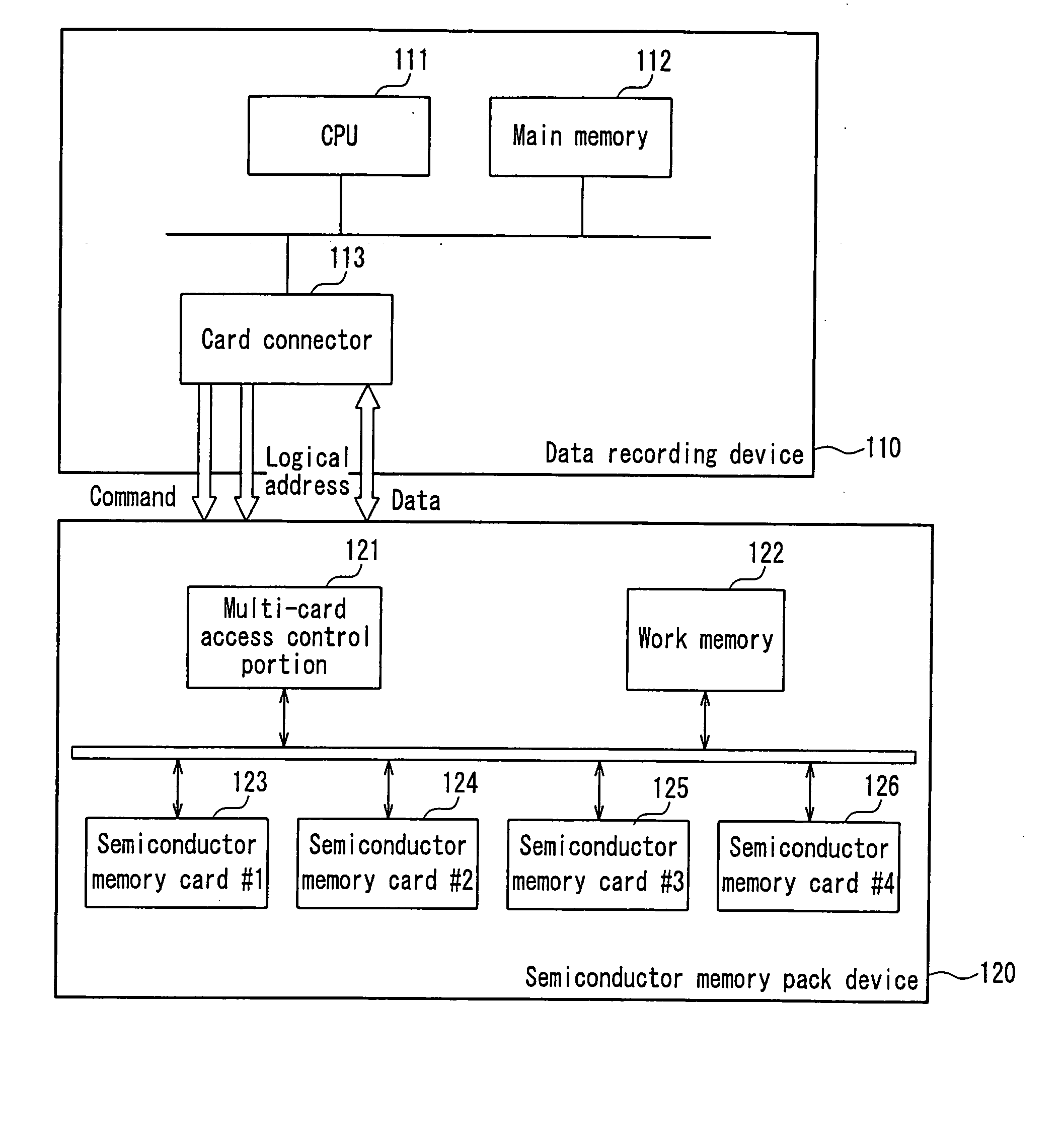
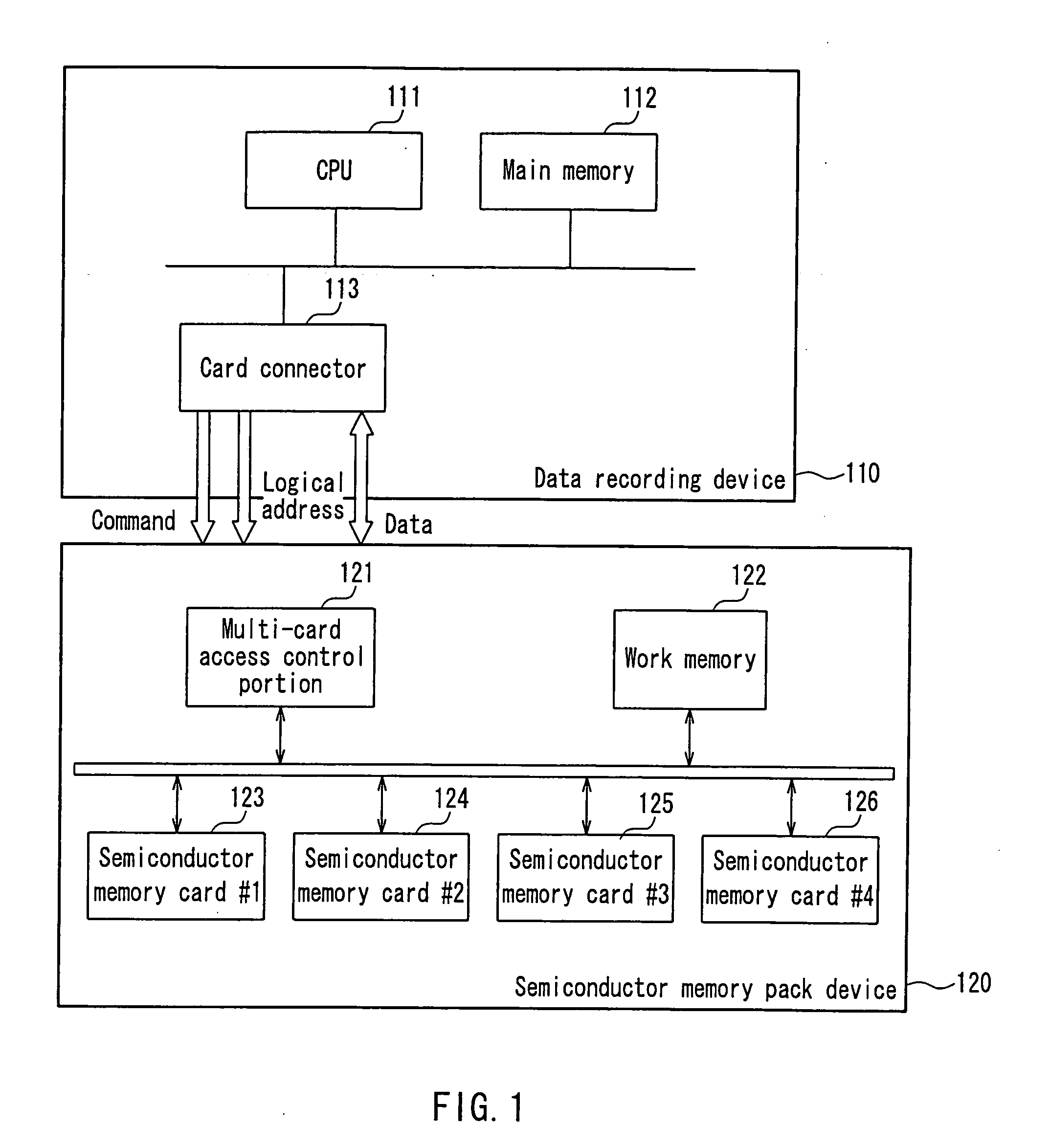
[0052] First, configurations of a data recording device according to an embodiment of the invention and a semiconductor memory pack device will be described with reference to FIG. 1. In FIG. 1, numeral 110 denotes a data recording device that gives an instruction to record data, and numeral 120 denotes a semiconductor memory pack device into which the data is recorded. The data recording device 110 is a device that records data into the semiconductor memory pack device 120, and may be a personal computer, a video camera, a disk recorder, or a digital camera, for example, although the data recording device 110 is not limited to these. The data recording device 110 is provided with such hardware as a CPU 111, a main memory 112, and a card connector 113. The CPU 111 performs arithmetic processing and controls an operation of the entire device. The main memory 112 temporarily stores data that is to be recorded into the semiconductor memory pack device 120, software that controls an oper...
embodiment 2
[0066] Another embodiment of the invention will be described with reference to FIGS. 1 and 4. The same numerals as Embodiment 1 are used for structures that serve a similar function as described in Embodiment 1, and detailed explanations of such structures are omitted.
[0067]FIG. 4 shows a state in which logical addresses of the four built-in semiconductor memory cards 123 to 126 are mapped to continuous logical addresses of the semiconductor memory pack device 120, and in which clusters, which are data management units of the file management portion 1109, are allocated to the continuous logical addresses of the semiconductor memory pack device 120. The four semiconductor memory cards 123 to 126 that are built into the semiconductor memory pack device 120 are interleaved in units of the erase block size (16 KB), are arranged in order from #1 to #4, and then are mapped to continuous logical addresses of the semiconductor memory pack device 120. Furthermore, since the four semiconduct...
embodiment 3
[0072] Subsequently, another embodiment of the invention will be described with reference to FIGS. 1 and 5. FIG. 5 shows a relationship of continuous logical addresses of the semiconductor memory pack device 120 and erase blocks (16 KB) of the four semiconductor memory cards 123 to 126 that are mapped to these logical addresses, and a cluster allocation when a data recording unit is set to four clusters (64 KB), which is a common multiple of the size obtained by adding up the sizes of the erase blocks (16 KB×4=64 K) of the semiconductor memory cards 123 to 126, and the size of one cluster (16 KB), which is a data management unit of the file management portion 1109.
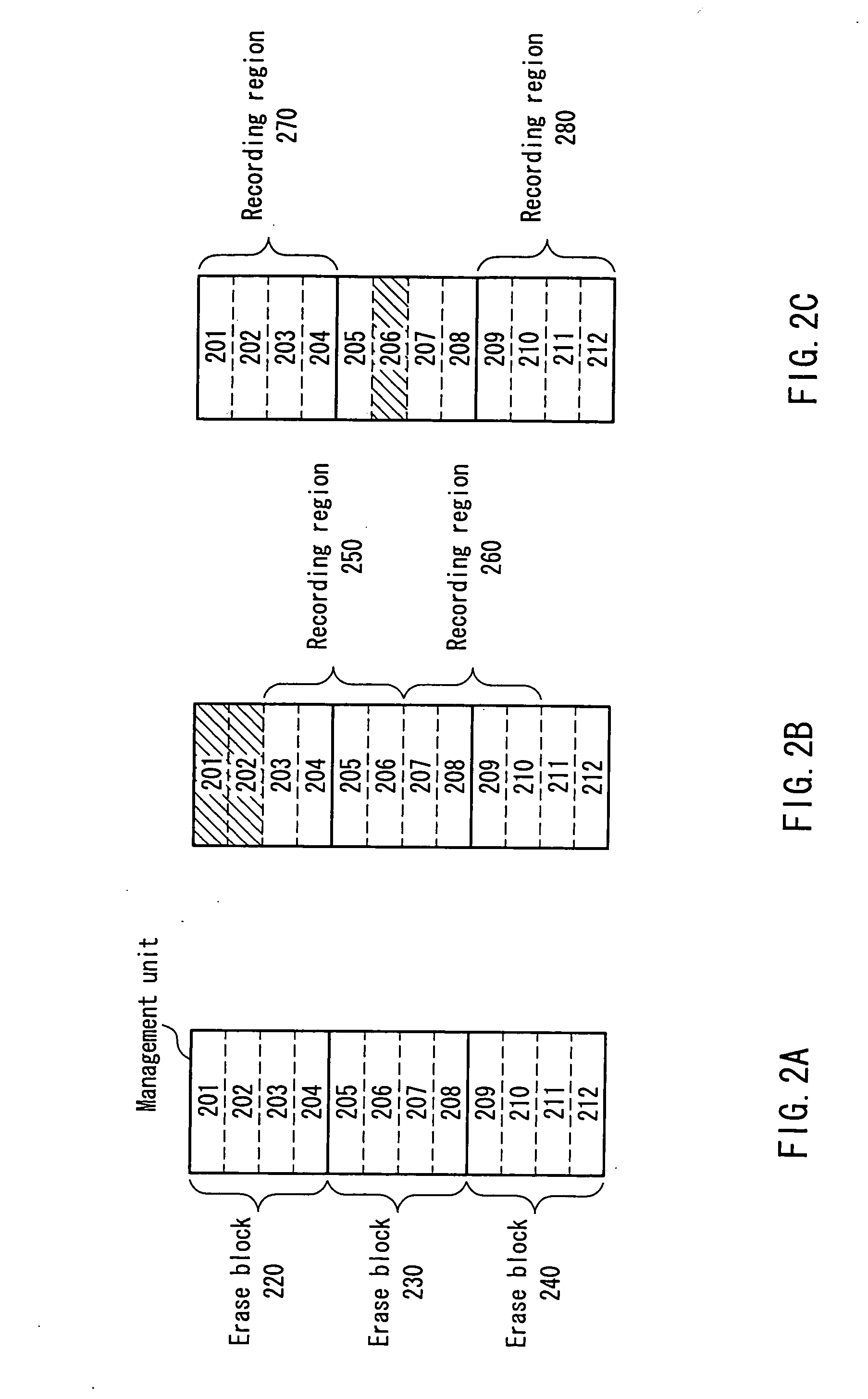
[0073] In conventional file systems, free regions are searched in units of clusters, which are the data management units. If there is a free region even for one cluster, data for one cluster is recorded at that logical address. However, in the file management portion 1109 of the data recording device 120 according to this...
PUM
 Abstract
Description
Claims
Application Information


