Integrated circuit structures for increasing resistance to single event upset

a technology of integrated circuits and events, applied in semiconductor devices, digital storage, instruments, etc., can solve problems such as memory cell “flipping”, memory cell error, and affected ic to malfunction, and achieve the effect of increasing the resistance to such an event, increasing the capacitance, and significantly increasing the capacitan

Inactive Publication Date: 2006-01-05
ALTERA CORP
View PDF11 Cites 15 Cited by
  • Summary
  • Abstract
  • Description
  • Claims
  • Application Information

AI Technical Summary

Benefits of technology

[0003] In accordance with this invention, an IC node that may be susceptible to SEU is given increased resistance to such an event by increasing its capacitance. Moreover, this capacitance preferably includes two portions. One portion includes having a first capacitor terminal connected to a source of relatively high or positive potential (e.g., VCC). A second portion includes having a second capacitor terminal connected to a source of relatively low or negative potential (e.g., VSS). The I

Problems solved by technology

The electrical charge(s) resulting from that ionization can flow to the electrical circuitry of the IC and cause errors in that circuitry.
A sufficiently rapid flow of a sufficiently large amount of electrical charge to that node as a result of an event like that descr

Method used


Image

  • Integrated circuit structures for increasing resistance to single event upset
  • Integrated circuit structures for increasing resistance to single event upset
  • Integrated circuit structures for increasing resistance to single event upset

Examples


Embodiment Construction

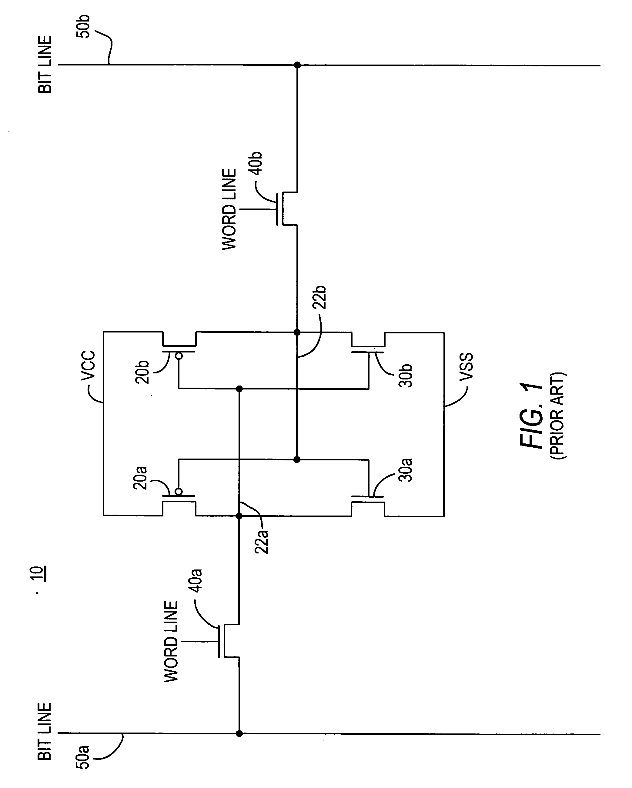
[0010]FIG. 1 shows a conventional static random access memory (“SRAM”) cell 10 of the type that may be used, for example, on a field programmable gate array (“FPGA”) IC. For example, cells of this type may be used to provide blocks of random access memory (so-called “user RAM”) on an FPGA. In cell 10, PMOS transistor 20a is connected in series with NMOS transistor 30a between a source of relatively high electrical potential VCC (or logic 1) and a source of relatively low electrical potential VSS (or logic 0 or ground). PMOS transistor 20b is similarly connected in series with NMOS transistor 30b between VCC and VSS. Node 22a is connected between transistors 20a and 30a and between the gates of transistors 20b and 30b. Node 22b is connected between transistors 20b and 30b and between the gates of transistors 20a and 30a. Node 22a is selectively connectable to bit line 50a via NMOS transistor 40a. Node 22b is selectively connectable to bit line 50b via NMOS transistor 40b.

[0011] When...


PUM


Abstract

A configuration memory cell (“CRAM”) for a field programmable gate array (“FPGA”) integrated circuit (“IC”) device is given increased resistance to single event upset (“SEU”). A portion of the gate structure of the input node of the CRAM is increased in size relative to the nominal size of the remainder of the gate structure. Part of the enlarged gate structure is located capacitively adjacent to an N-well region of the IC, and another part is located capacitively adjacent to a P-well region of the IC. This arrangement gives the input node increased capacitance to resist SEU, regardless of the logical level of the input node. The invention is also applicable to any node of any type of memory cell for which increased resistance to SEU is desired.

Description

BACKGROUND OF THE INVENTION [0001] This invention relates to integrated circuit (“IC”) devices, and more particularly IC structures that increase the resistance of the IC to certain kinds of memory errors due to such causes as alpha particles and atmospheric neutrons. [0002] An event such as an alpha particle or atmospheric neutron travelling through the material of an IC can cause ionization of that material in the vicinity of the event. The electrical charge(s) resulting from that ionization can flow to the electrical circuitry of the IC and cause errors in that circuitry. For example, a memory cell may depend on a node of the memory cell remaining at a certain electrical potential (voltage) in order for the memory cell to hold a stored data value. A sufficiently rapid flow of a sufficiently large amount of electrical charge to that node as a result of an event like that described above may cause the node to deviate from the required potential and thereby cause the memory cell to ...

Claims


Application Information

Patent Timeline
IPC IPC(8): H01L29/739H01L27/10G11C16/04G11C11/34
CPCG11C11/412H01L27/11807H01L27/0207
Inventor SIDHU, LAKHBEER S.RAHIM, IRFANWATT, JEFFREYTURNER, JOHN E.
Owner ALTERA CORP
Why Eureka
Try Eureka