Direct connection multi-chip semiconductor element structure

a semiconductor element and multi-chip technology, applied in semiconductor devices, semiconductor/solid-state device details, electrical apparatus, etc., can solve the problems of increasing fabrication costs, limiting the layout of substrates, and complex electrically conductive paths, so as to reduce the overall thickness of semiconductor devices, improve electrical performance, and facilitate fabrication flexibility

Active Publication Date: 2006-01-05
PHOENIX PRECISION TECH CORP
View PDF8 Cites 111 Cited by
  • Summary
  • Abstract
  • Description
  • Claims
  • Application Information

AI Technical Summary

Benefits of technology

[0018] Therefore, the direct connection multi-chip semiconductor element structure in the present invention has a plurality of semiconductor chips being mounted on a heat sink, such that heat generated by the semiconductor chips during operation can be effectively dissipated via the beat sink, and the heat sink also provides an electromagnetic shielding effect for the semiconductor chips. The semiconductor element structure incorporated with the plurality of semiconductor chips allows multiple chips to be integrated in a circuit board, thereby reducing the overall thickness of the semiconductor device to meet the size miniaturization requirement. Moreover, the direct connection multi-chip semiconductor element structure in the present invention facilitates direct extension of a circuit structure from the plurality of semiconductor chips to provide direct electrical extension for the semiconductor chips, thereby improving electrical performance for an electronic device having the semiconductor element structure. And exposed electrical connection terminals can be formed in the circuit structure extended from the chips, so as to achieve electrical connection between the semiconductor element structure and an external electronic device.
[0019] Furthermore, the direct connection multi-chip semiconductor element structure in the present invention incorporates the heat sink, the semiconductor chips, and the circuit structure, such that the chip-carrier fabrication processes and the semiconductor packaging processes can be combined to provide more flexibility in fabrication according to a client's requirement, and the semiconductor fabrication processes can be simplified, as well as the interface integration problem can be solved, unlike the complex fabrication processes and equipment required in the prior art for electrically connecting a semiconductor chip to a circuit board via wire-bonding or flip-chip technology or even to an external electronic device, such that the quality and reliability of the semiconductor device can be effectively improved in the present invention.

Problems solved by technology

This not only sets a limitation on the substrate layout but also requires high-density fabrication processes to form the pads, thereby increasing the fabrication cost.
Additionally, since the electrical connection between the semiconductor chips in the semiconductor device is established through the bonding wires, the solder balls, and circuits of the substrate, such electrically conductive path is very complex and makes the electrical performances hard to be improved.
However, the foregoing semiconductor device having the plurality of stacked semiconductor packages has significant drawbacks.
In other words, electrically-connecting areas on the substrate of each of the stacked semiconductor package are restricted, thereby affecting the trace routability of the substrate, and the number and distribution of input / output (I / O) connections of the overlying semiconductor packages are also restricted, making the design flexibility of the entire semiconductor device undesirably reduced.
Further, the plurality of semiconductor packages must formed before performing the stacking process, such that the overall fabrication processes are complex and the fabrication time and cost are increased.
Moreover, the electrical connection between the semiconductor chips of the stacked semiconductor packages is still achieved via the substrate circuits and the solder balls of each of the semiconductor packages, such electrically conductive path is very complex and makes the electrical performances hard to be improved.
Therefore, such fabrication processes of the semiconductor device, involving different manufacturers such as chip-carrier manufacturers and semiconductor packaging manufacturers, are complicated and usually cause difficulty in interface integration.
In case the client intends to alter the functional design of the semiconductor device, it would involve further complex change and interface integration, such that the flexibility in alteration and the economical effects cannot be achieved.

Method used


Image

  • Direct connection multi-chip semiconductor element structure
  • Direct connection multi-chip semiconductor element structure
  • Direct connection multi-chip semiconductor element structure

Examples


Embodiment Construction

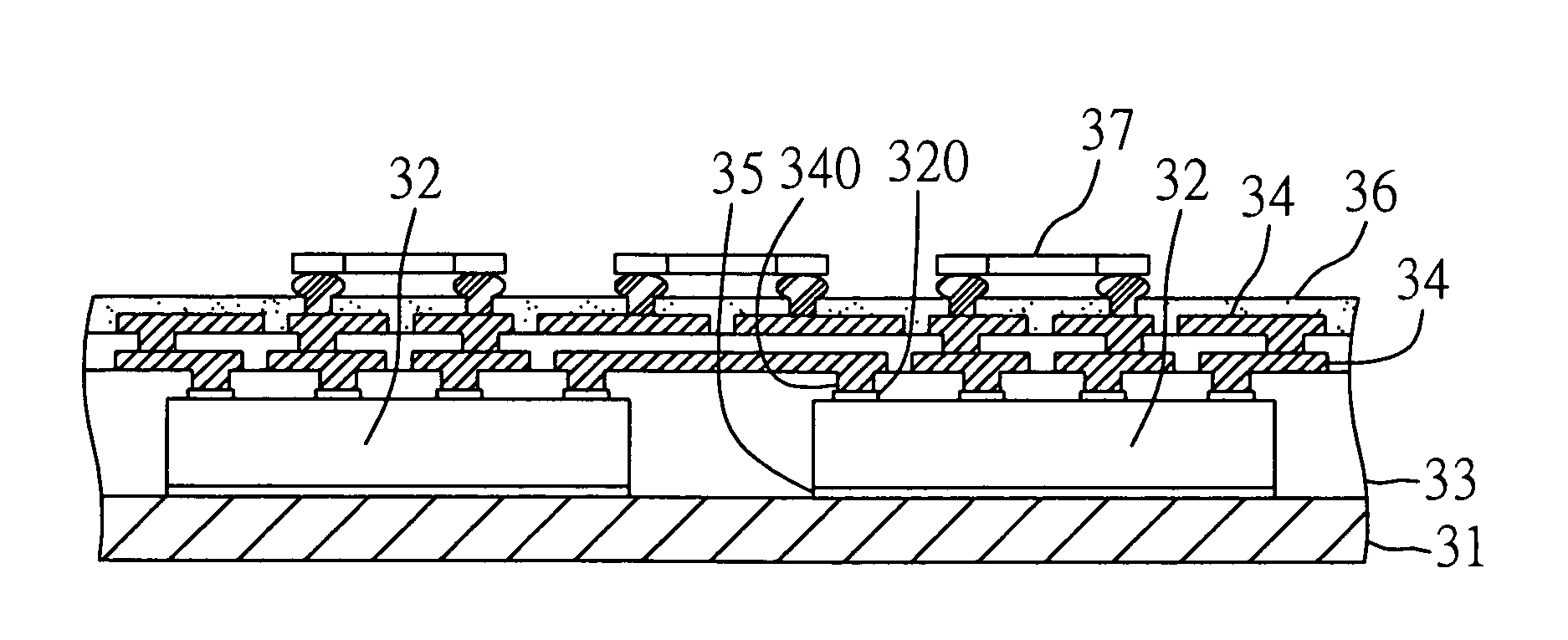
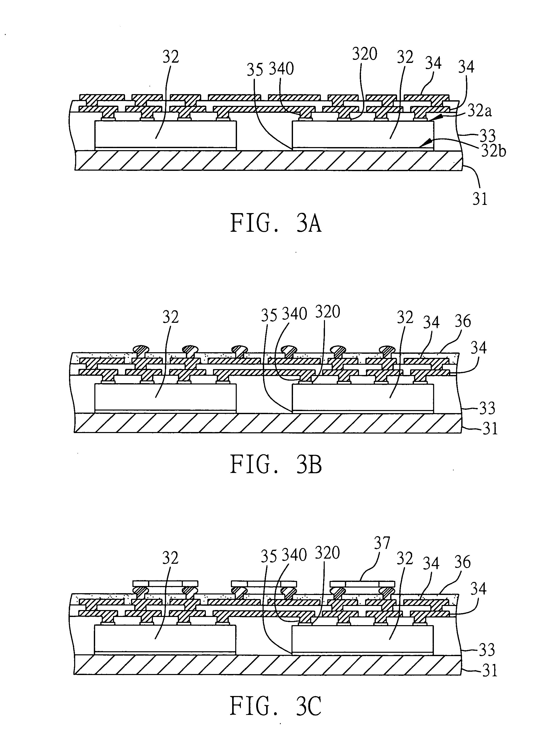
[0027]FIGS. 3A and 3B show cross-sectional views of a direct connection multi-chip semiconductor element structure according to the present invention.

[0028] Referring to FIG. 3A, the direct connection multi-chip semiconductor element structure proposed in the present invention comprises a heat sink 31; a plurality of semiconductor chips 32 mounted on the heat sink 31; at least one insulating layer 33 formed on a surface of the heat sink 31 mounted with the semiconductor chips 32; and at least one patterned circuit layer 34 formed on the insulating layer 33. The patterned circuit layer 34 is electrically connected to the semiconductor chips 32 via a plurality of conductive means 340 formed in the insulating layer 33, and also allows a part of the semiconductor chips 32 to be electrically interconnected.

[0029] The heat sink 31 can be made of a metal plate for carrying the plurality of semiconductor chips 32, or comprises a plurality of metal plates provided only at areas for carryin...


PUM


Abstract

A direct connection multi-chip semiconductor element structure is proposed. A plurality of semiconductor chips are mounted and supported on a metal heat sink, such that heat generated by the chips during operation can be dissipated via the heat sink. A circuit structure is extended from the chips to provide direct electrical extension for the chips and improve the electrical performances. And exposed electrical connection terminals can be formed in the circuit structure extended from the chips to be directly electrically connected to an external electronic device.

Description

FIELD OF THE INVENTION [0001] The present invention relates to direct connection multi-chip semiconductor element structures, and more particularly, to a semiconductor element structure integrated with a plurality of semiconductor chips, which can directly provide external electrical connection for the semiconductor chips. BACKGROUND OF THE INVENTION [0002] Along with electronic products being developed toward having multi-functionality, high performances and high operating speed, semiconductor manufacturers have endeavored to provide a multi-chip module (MCM) for incorporating a plurality of chips in a semiconductor device to meet the above requirements for the electronic products. [0003] U.S. Pat. No. 6,303,997 discloses a semiconductor device integrated with a plurality of chips. Referring to FIG. 1, on an upper surface of a substrate 10 there are provided a semiconductor chip 11 electrically connected to the substrate 10 and a fabricated BGA (ball grid array) semiconductor packa...

Claims


Application Information

Patent Timeline
Patent Type & Authority Applications(United States)
IPC IPC(8): H01L23/10H01L23/31H01L23/36H01L23/538H01L25/065
CPCH01L23/36H01L24/48H01L24/24H01L24/82H01L25/0655H01L2224/16145H01L2224/24137H01L2224/24226H01L2224/32225H01L2224/48091H01L2224/48227H01L2224/73265H01L2224/73267H01L2924/01029H01L2924/01078H01L2924/01079H01L2924/14H01L2924/15192H01L2924/15311H01L2924/19041H01L2924/19042H01L2924/19043H01L2924/3025H01L2224/32245H01L2224/16225H01L2924/014H01L2924/01047H01L2924/01006H01L23/5389H01L2924/00014H01L2924/00H01L2224/04105H01L2224/12105H01L2924/181H01L2924/00012H01L2224/45099H01L2224/45015H01L2924/207
Inventor HU, CHU-CHIN
Owner PHOENIX PRECISION TECH CORP
Why Eureka
Try Eureka