Organic element for electroluminescent devices

Active Publication Date: 2006-01-05
GLOBAL OLED TECH
View PDF3 Cites 34 Cited by
  • Summary
  • Abstract
  • Description
  • Claims
  • Application Information

AI Technical Summary

Benefits of technology

[0018] The invention also provides lighting devices containing the EL device and light emitting processes employi

Problems solved by technology

While organic electroluminescent (EL) devices have been known for over two decades, their performance limitations have represented a barrier to many desir

Method used


Image

  • Organic element for electroluminescent devices
  • Organic element for electroluminescent devices
  • Organic element for electroluminescent devices

Examples


example 1

DEVICE EXAMPLE 1

EL Device Fabrication of Samples 1-5

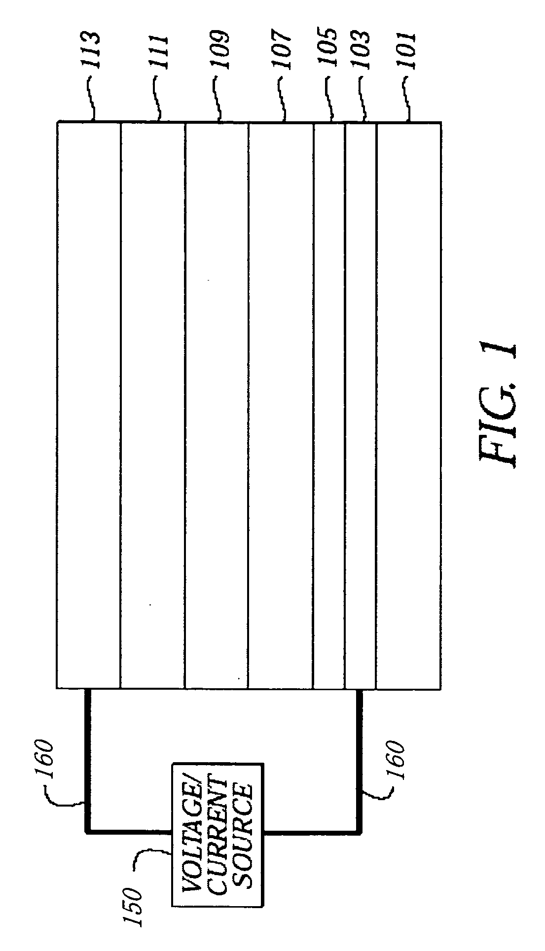
[0183] An EL device (Sample 1) satisfying the requirements of the invention was constructed in the following manner: [0184] 1. A glass substrate coated with an 85 nm layer of indium-tin oxide (ITO) as the anode was sequentially ultrasonicated in a commercial detergent, rinsed in deionized water, degreased in toluene vapor and exposed to oxygen plasma for about 1 min. [0185] 2. Over the ITO was deposited a 1 nm fluorocarbon (CFx) hole-injecting layer (HIL) by plasma-assisted deposition of CHF3. [0186] 3. A hole-transporting layer (HTL) of N,N′-di-1-naphthyl-N,N′-diphenyl-4,4′-diaminobiphenyl (NPB) having a thickness of 75 nm was then evaporated from a tantalum boat. [0187] 4. A 20.0 nm light-emitting layer (LEL) of 2-t-butyl-9,10-di-(2-naphthyl)anthracene (tBADN) and including the boron complex light-emitting material, BD-7, at a level of 2% by volume of the LEL layer, and also including the stilbene compound, Inv-5, at a level of ...

example 2

DEVICE EXAMPLE 2

EL Device Fabrication of Comparative Samples 6-10

[0193] An EL device (Sample 6) was fabricated in the same manner as Sample 1, except the boron complex light-emitting material, BD-7, was replaced with light-emitting material ST-1 at a level of 2 volume %. Samples 7-9, incorporating Inv-5 and ST-1 were fabricated in an identical manner as Sample 6 except Inv-5 was used at the levels indicated in the Table 2. Sample 10 was constructed in the same manner as Sample 6 except Inv-5 was omitted.

[0194] Device Samples 6-10 were tested for efficiency and color at an operating current of 20 mA / cm2 and the results are reported in Table 2 in the form of CIE coordinates, efficiency (W / A), and the percent increase in efficiency relative to Sample 10 which did not contain Inv-5.

TABLE 1Testing Results For Samples 1-5.Inv-5EfficiencyIncrease inSampleTypeLevel (%)CIExCIEyW / AEfficiency1Inventive0.500.1500.2320.06013%2Inventive1.000.1490.2290.06319%3Inventive1.500.1480.2300.06523%4In...


PUM

PropertyMeasurementUnit
Percent by volumeaaaaaaaaaa
Timeaaaaaaaaaa

Abstract

An electroluminescent device includes a light-emitting layer containing a host material and: (a) a compound of Formula (1):
X1—Ar1—C(R1)═C(R2)—Ar2   (1)
wherein:
Ar1 represents a divalent aromatic group;
Ar2 represents an aromatic group;
X1 represents at least one electron-donating group;
R1 and R2 independently represent hydrogen or a substituent; and (b) a light-emitting boron complex having an absorption spectrum that overlaps with the emission spectrum of compound (1). The device serves to improve luminance efficiency while maintaining good color purity.

Description

FIELD OF THE INVENTION [0001] This invention relates to an electroluminescent (EL) device comprising a light-emitting layer containing a stilbene derivative and a boron complex, which affords high luminance. BACKGROUND OF THE INVENTION [0002] While organic electroluminescent (EL) devices have been known for over two decades, their performance limitations have represented a barrier to many desirable applications. In simplest form, an organic EL device is comprised of an anode for hole injection, a cathode for electron injection, and an organic medium sandwiched between these electrodes to support charge recombination that yields emission of light. These devices are also commonly referred to as organic light-emitting diodes, or OLEDs. Representative of earlier organic EL devices are Gurnee et al. U.S. Pat. No. 3,172,862, issued Mar. 9, 1965; Gurnee U.S. Pat. No. 3,173,050, issued Mar. 9, 1965; Dresner, “Double Injection Electroluminescence in Anthracene”, RCA Review, 30, 322-334, (196...

Claims


Application Information

Patent Timeline
IPC IPC(8): H05B33/14
CPCC09K11/06Y10S428/917C09K2211/1014C09K2211/1029C09K2211/1033C09K2211/1037C09K2211/1055C09K2211/107C09K2211/1088C09K2211/181C09K2211/186C09K2211/188H01L51/0052H01L51/0059H01L51/006H01L51/0062H01L51/0071H01L51/0073H01L51/0079H01L51/008H01L51/0081H01L2251/308H05B33/14C09K2211/1011H10K85/615H10K85/649H10K85/631H10K85/633H10K85/657H10K85/6574H10K85/321H10K85/322H10K85/324H10K2102/103
Inventor HELBER, MARGARET J.RICKS, MICHELE L.NICHOLS, WILLIAM F.MATOCHIK, THOMAS L.VREELAND, WILLIAM B.DONOVAN, KEVIN M.
Owner GLOBAL OLED TECH
Why Eureka
Try Eureka