

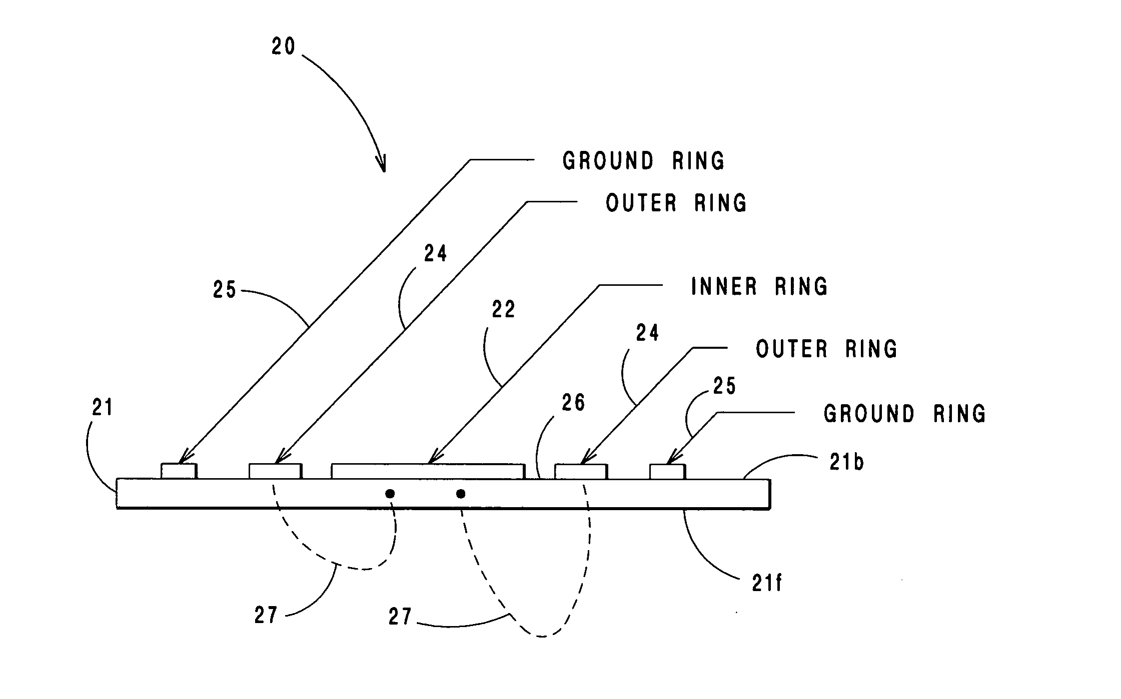
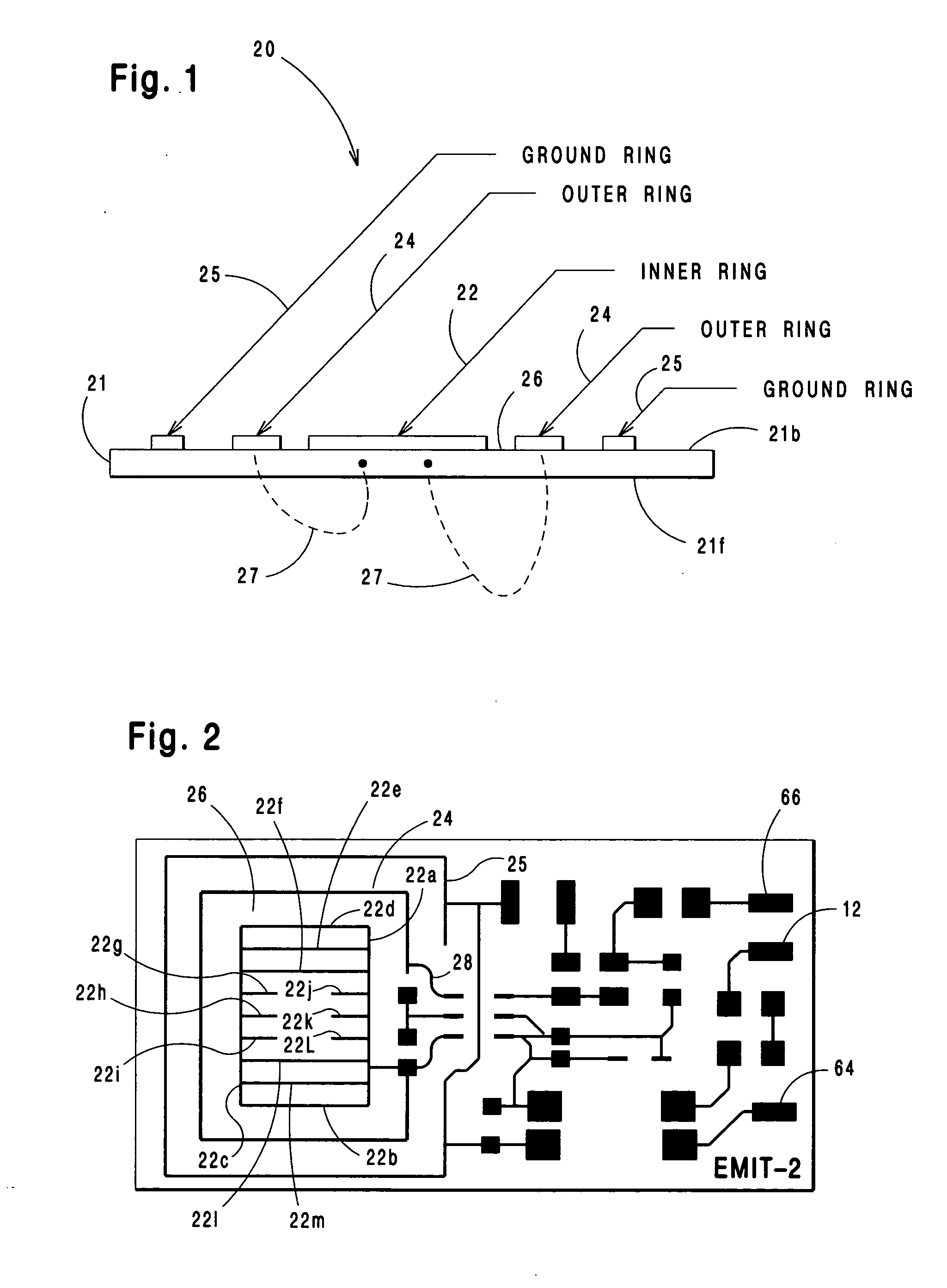
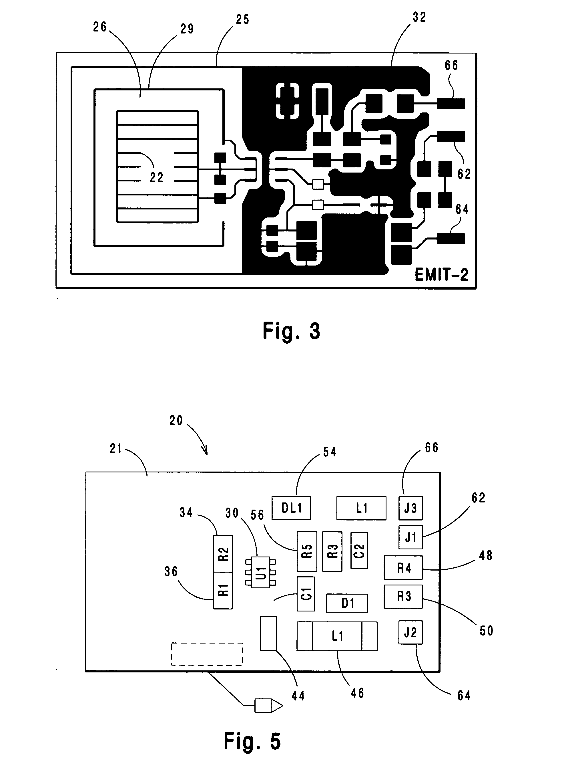
EMI resistant balanced touch sensor and method
a balanced, touch sensor technology, applied in the direction of electronic switching, pulse technique, instruments, etc., can solve the problems of tao electrode damage, touch panel cost and complexity increase, tao electrode damage, etc., to reduce the difference in signal level, improve electromagnetic immunity, and less expensive
- Summary
- Abstract
- Description
- Claims
- Application Information
AI Technical Summary
Benefits of technology
Problems solved by technology
Method used
Image

Examples
second embodiment
[0060] In a second embodiment best seen in FIGS. 6, 7 and 8, both sides of a two-sided printed circuit board 68 make a double-sided balanced electrode pattern 69 having first electrode traces 70 on a first side of PCB 68 opposite second electrode traces 72 on the second side of PCB 68. As best seen in FIGS. 6, 7 and 8, double-sided balanced electrode pattern 69 includes a component side layout (best seen in FIG. 7) with conductive traces for the second electrode 72 in evenly spaced lines on one side of PCB 68; the lines are separated by evenly spaced non-conductive channels 73. FIG. 8 shows the other side of PCB 68 carrying conductive traces for the first electrode 70 in evenly spaced lines, and showing the non-conductive channels 71 between the traces. The side elevational view of FIG. 6 shows that the electrode patterns are offset slightly so that each first electrode conductive trace 70 is positioned opposite a second side non-conductive channel segment 73 and between adjacent se...
third embodiment
[0061] In a third embodiment best seen in FIGS. 9a and 9b, flat balanced pad sensor electrode pattern 78 includes a first electrode pad 80 situated on one side of a PCB and alongside a second electrode 82. FIG. 9a illustrates flat balanced pad sensor electrode pattern 78 with offset electrodes 80, 82. FIG. 9b shows a cross section side elevation view of the flat balanced pad sensor electrode pattern 78 with offset electrodes 80, 82 and a three sided or U-shaped ground ring 84. First electrode 80 and second electrode 82 are thin traces of conductive material of substantially surface equal area. As with the embodiments described above, first electrode 80 is connected via a first biasing or tuning resistor 34 to sensor IC 30 and second electrode 82 is connected via a second biasing or tuning resistor 36 to sensor IC 30.
[0062] Other embodiments using the two sided PCB are also suitable for use in a variety of applications. FIGS. 10, 11 and 12 illustrate a balanced pad sensor electrode p...
PUM
 Abstract
Description
Claims
Application Information