Circuits and methods for recovering a clock signal

a clock signal and circuit technology, applied in the field of circuits and methods for recovering clock signals, can solve the problems of increasing chip area, increasing power consumption, and difficulty in designing a complementary metal oxide semiconductor (cmos)

Active Publication Date: 2006-01-12
SAMSUNG ELECTRONICS CO LTD
View PDF7 Cites 46 Cited by
  • Summary
  • Abstract
  • Description
  • Claims
  • Application Information

AI Technical Summary

Benefits of technology

[0016] Another example embodiment of the present invention is directed to a circuit for recovering a clock signal and data. The circuit may include a frequency multiplier generating a plurality of local clock signals from a plurality of received global clock signals, the local clock signals at a frequency higher than a frequency of the received global clock signals, and a phase interpolator generating a recovered clock signal based on the generated local clock signals. The circuit may include a phase shifter adjusting the phase of the recovered clock signal so as to synchronize the phase of the recovered clock signal with a phase of input data that is input to the phase shifter, and generating recovered data based on the synchronized recovered clock signal.
[0017] Another example embodiment of the present invention is directed to a method for recovering a clock signal and data. In the method, a plurality of local clock signals may be generated from a plurality of received global clock signals. The local clock signals may be generated at a frequency higher than a frequency of the received global clock signals. A recovered clock signal may

Problems solved by technology

Using two PLLs may increase a chip area and also may increase power consumption.
Thus, when the data rate is increased, the use of a single PLL configuration for a CDR circuit may lead to difficulties in designing a complementary metal oxide semiconductor (CMOS) of a PLL/VCO having low jitter characteristics.
Moreover, power consumption of the transmission buffer may be increased.
However, it may be difficult to implement a VCO which generates a frequency in excess of 8 GHz, and which simultaneously satisfies operational reliability, based on the present CMOS technology.
Therefore, as data rate increases, it may be difficult to design a low jitter CMOS in a PLL, a

Method used


Image

  • Circuits and methods for recovering a clock signal
  • Circuits and methods for recovering a clock signal
  • Circuits and methods for recovering a clock signal

Examples


Embodiment Construction

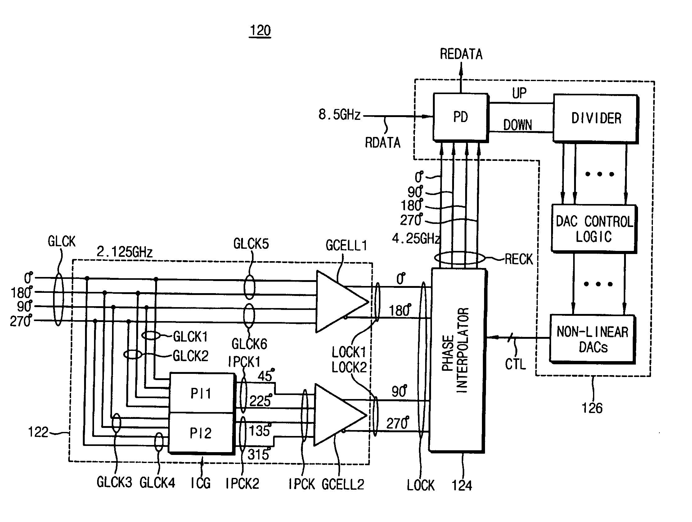
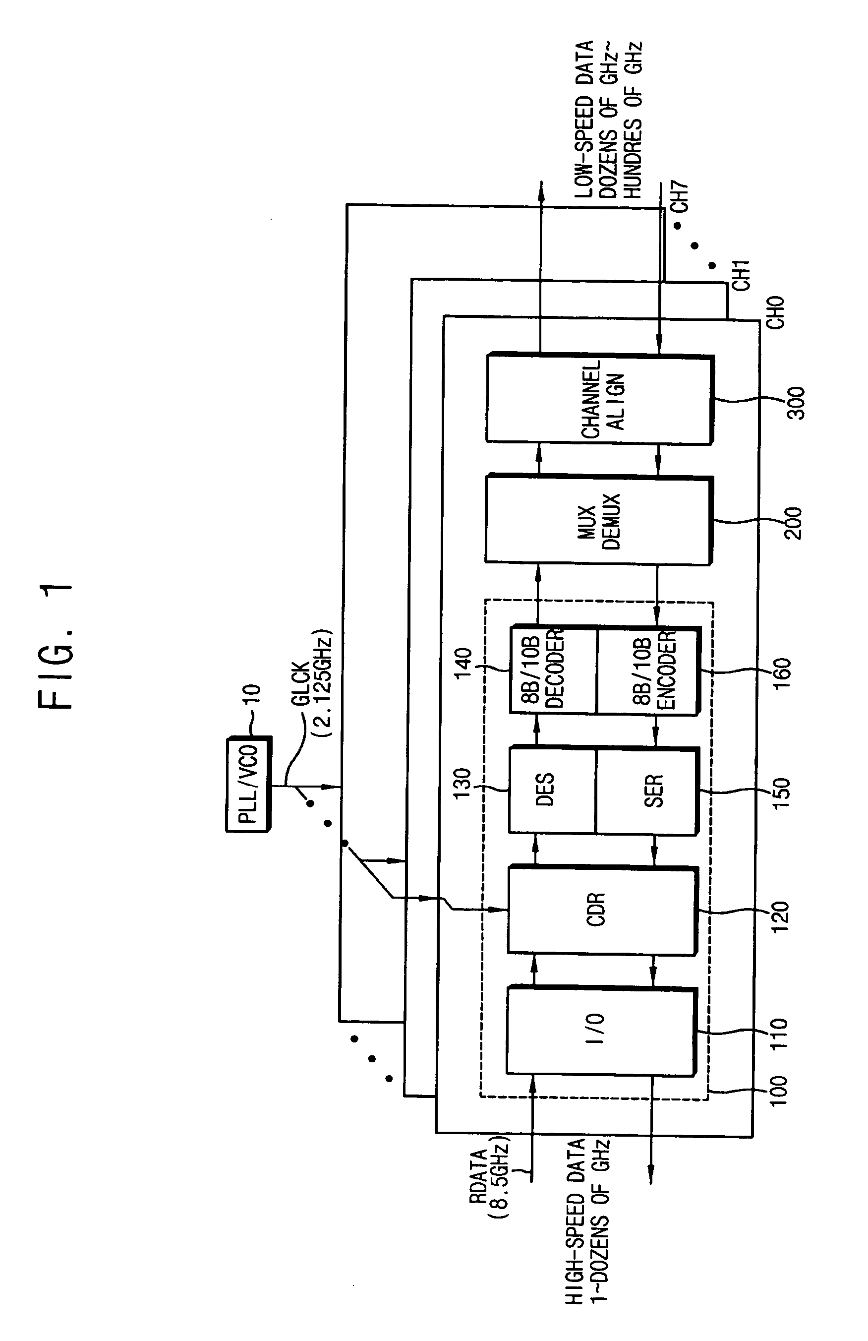
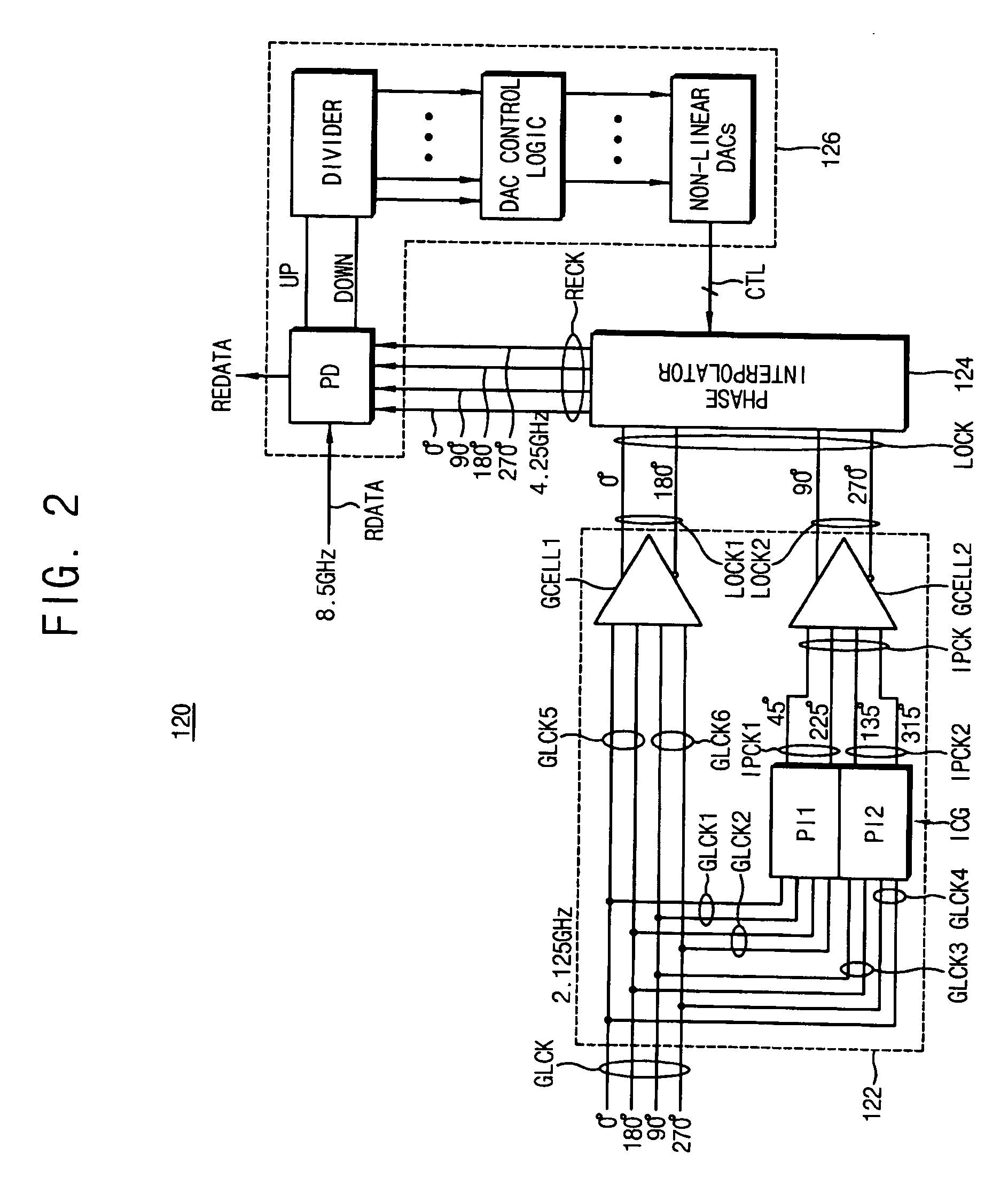
[0028] Detailed illustrative example embodiments of the present invention are disclosed herein. However, specific structural and functional details disclosed herein are merely representative for purposes of describing example embodiments of the present invention. The invention may, however, be embodied in many alternative forms and should not be construed as limited to the example embodiments set forth herein. Example embodiments of the present invention may thus cover all modifications, equivalents and alternatives falling within the spirit and scope of the present invention. Like numbers refer to like elements throughout the description of the figures.

[0029] It should also be noted that in some alternative implementations, the functions / acts noted in the blocks may occur out of the order noted in the flowcharts. For example, two blocks shown in succession may in fact be executed substantially concurrently or the blocks may be executed in the reverse order, depending upon the func...


PUM


Abstract

A circuit for recovering a clock signal may include a frequency multiplier configured to generate a plurality of local clock signals, each having a different phase, based on a plurality of received global clock signals at a first frequency and each having a different phase. The local clock signals may be generated at a second frequency higher than the first frequency. The circuit may include a phase interpolator configured to generate a recovered clock signal at a given phase and at a third frequency, based on the generated local clock signals, and a phase shifter configured to adjust the phase of the recovered clock signal so as to synchronize the phase of the recovered clock signal with a phrase of input data that is input to the phase shifter.

Description

CLAIM FOR PRIORITY [0001] This application claims priority to Korean Patent Application No. 2004-52171 filed on Jul. 6, 2004 in the Korean Intellectual Property Office (KIPO), the entire contents of which are hereby incorporated by reference. BACKGROUND OF THE INVENTION [0002] 1. Field of the Invention [0003] The present invention relates, in general, to circuits and methods for recovering a clock signal. [0004] 2. Description of the Related Art [0005] In general, a clock and data recovery (CDR) circuit provides a clock signal that is used to restore digital signals in a receiver stage of a high-speed data communication system such as an optical communication system, a backplane routing system and / or a chip-to-chip interconnect system, for example. The CDR circuit may recover a clock signal using a reference clock signal provided from a crystal oscillator, or alternatively may recover a clock signal without using a reference clock signal. When a reference clock signal is used to rec...

Claims


Application Information

Patent Timeline
IPC IPC(8): H04L25/00
CPCH03L7/0812H04L7/0338H04L7/0025H04L7/02
Inventor KIM, NYUN-TAEKIM, KI-HONGUEDA, KIMIOWANG, SHU-JIANGKIM, MI-JEONG
Owner SAMSUNG ELECTRONICS CO LTD
Why Eureka
Try Eureka