Display device mounted with read function and electric appliance

a display device and function technology, applied in the direction of static indicating devices, acquiring/reconfiguring fingerprints/palmprints, instruments, etc., can solve the problems of inability to read out information on the object to be read out correctly, image expressed by a correct gray-scale becomes difficult to be displayed, and the desired color cannot be obtained. , to achieve the effect of improving white balance, improving luminance of each color, and high resolution

Inactive Publication Date: 2006-01-19
SEMICON ENERGY LAB CO LTD
View PDF26 Cites 69 Cited by
  • Summary
  • Abstract
  • Description
  • Claims
  • Application Information

AI Technical Summary

Benefits of technology

[0025] The display device mounted with a read function according to the present invention can read out correctly information on an object to be read out since a bank layer has a light-shielding property capable of preventing extra light from entering an image pick-up element.
[0026] The variation of luminance of each color can be improved by varying the area of ea...

Problems solved by technology

When white balance becomes dulled, desired color cannot be obtained and an image expressed by a correct gray-scale becomes difficult to be displayed.
When such the extra light enters the image pick-up element, information...

Method used


Image

  • Display device mounted with read function and electric appliance
  • Display device mounted with read function and electric appliance
  • Display device mounted with read function and electric appliance

Examples


embodiment 1

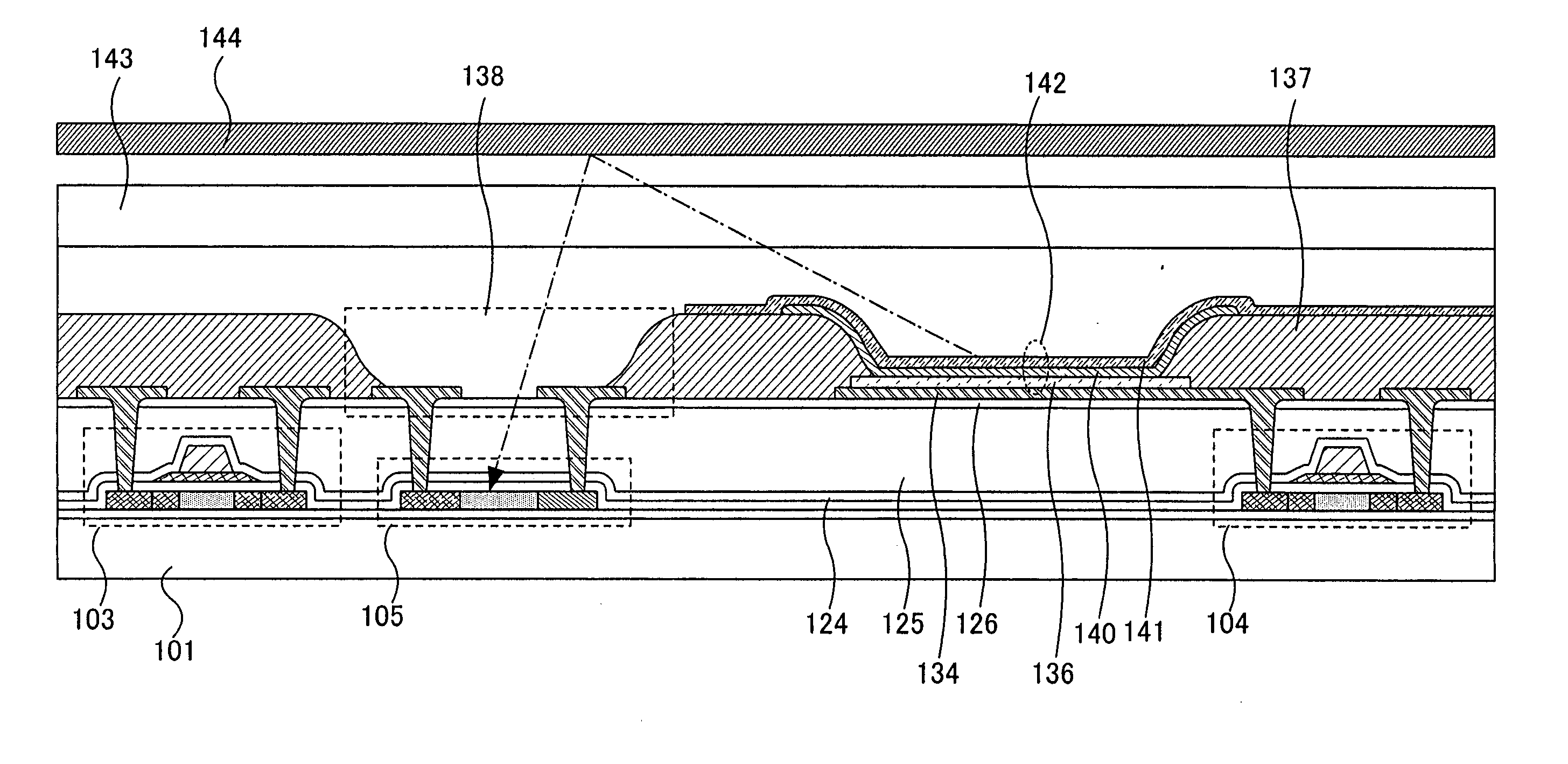
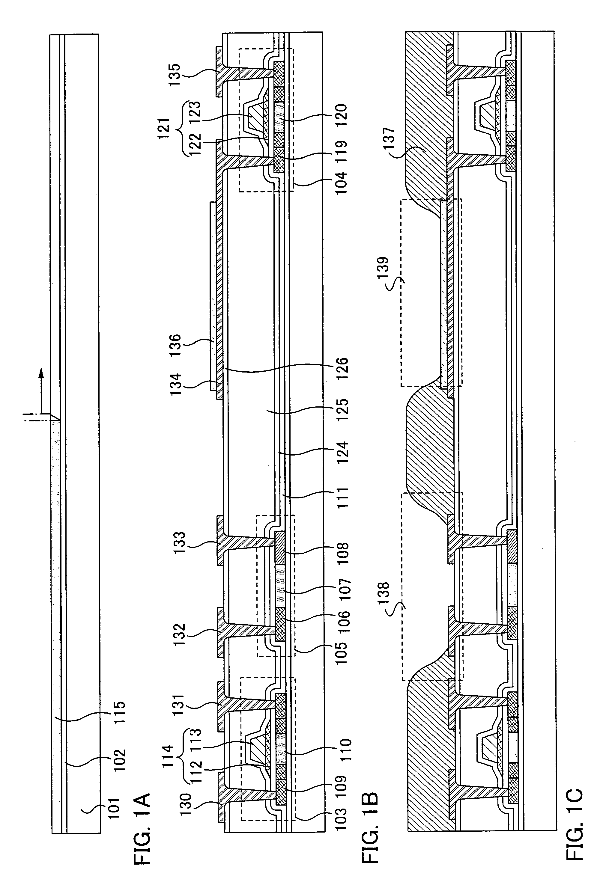
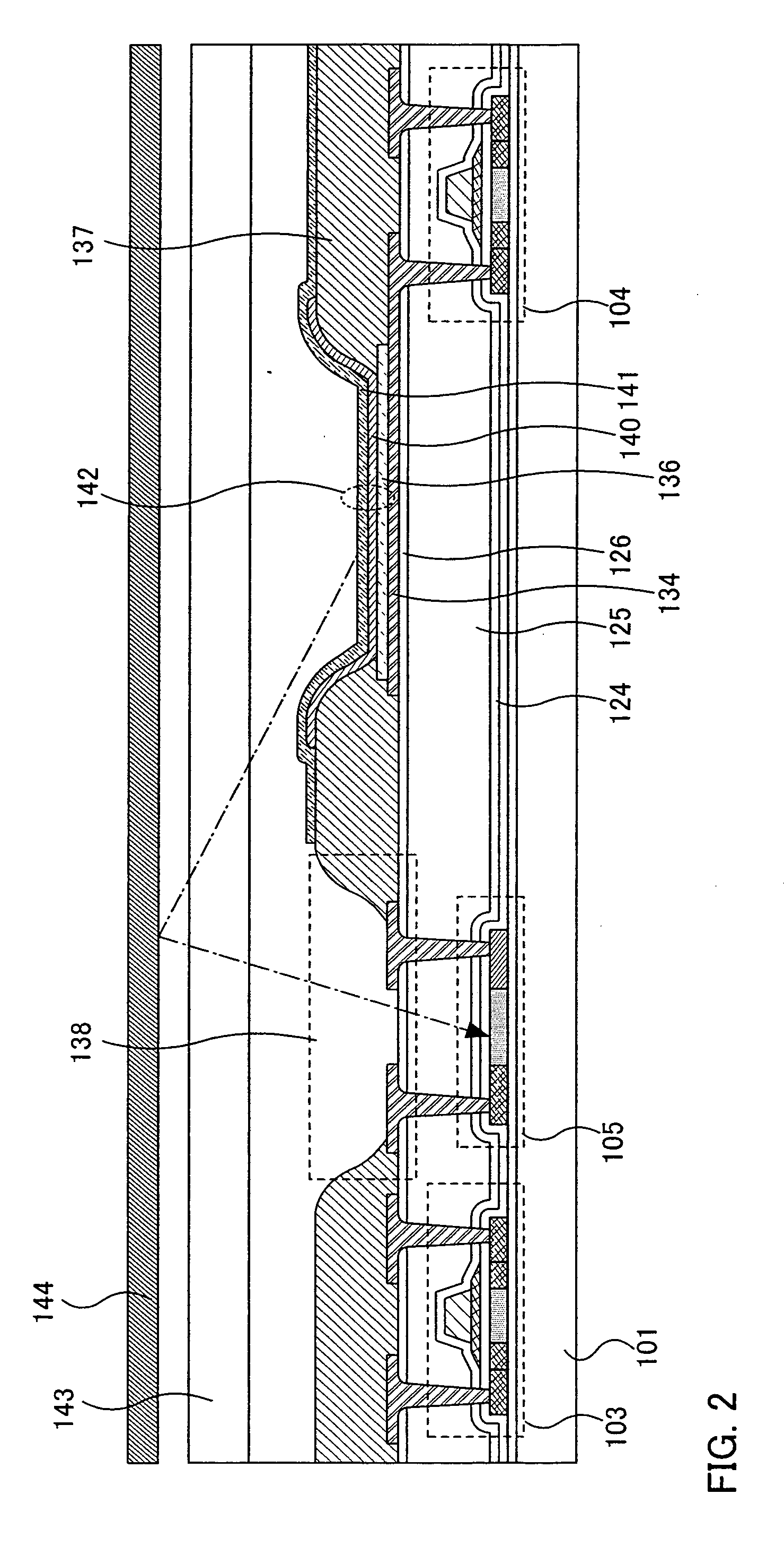
[0042] In order to explain the structure of a display device mounted with a read function, the manufacturing process thereof is firstly explained.

[0043] An insulating layer 102 serving as a base layer is formed over a substrate 101 having an insulating surface (FIG. 1A). As the substrate 101, a glass substrate, a quartz substrate, a silicon substrate, or a plastic substrate having heat resistance that can withstand process temperature is used.

[0044] An amorphous semiconductor layer is formed on the insulating film 102 by a known method (a sputtering method, a plasma CVD method, or the like). Then, a crystalline semiconductor layer 115 is formed by crystallizing the amorphous semiconductor layer by a known crystallization method (a laser crystallization method, a thermal crystallization method, a thermal crystallization method using a catalyst such as nickel).

[0045] Then, the crystallization semiconductor layer 115 is pattern processed to form an island-like crystalline semiconduc...

embodiment 2

[0081] As noted above, a pixel 206 included in a display device mounted with a read function according to the present invention has a plurality of sub pixels composed of at least one sub pixel with a light-emitting element and one sub pixel with an image pick-up element. Hereinafter, the structure of the display device mounted with a read function characterized in varying the area of the sub pixel provided over a substrate.

[0082] The first structure of the display device mounted with a read function is explained with reference to the drawings. The pixel 206 may be formed to include a first sub pixel 211 with a light-emitting element exhibiting red emission, a second sub pixel 212 with a light-emitting element exhibiting green emission, a third sub pixel 213 with a light-emitting element exhibiting blue emission, and a fourth sub pixel 214 with an image pick-up element (FIGS. 6A to 6E). Over the substrate, the area of the first sub pixel 211 is the same or approximately the same as ...

example 1

[0087] A pixel 206 included in a display device mounted with a read function according to the present invention has a plurality of sub pixels composed of one sub pixel having at least a light-emitting element and one sub pixel having an image pick-up element. Here, an example of an equivalent circuit of the pixel 206 is explained with reference to the drawings.

[0088] Firstly, the equivalent circuit in the case that the pixel 206 has a first sub pixel 211 having a first light-emitting element exhibiting red emission, a second sub pixel 212 having a second light-emitting element exhibiting green emission, a third sub pixel 213 having a third light-emitting element exhibiting blue emission, and a fourth sub pixel 214 having an image pick-up element is explained (FIG. 8).

[0089] Each of the first sub pixel 211 to the third sub pixel 213 has a switch transistor 250, a drive transistor 251, a capacitor element 252, and a light-emitting element 253 in a region surrounded by a source line ...


PUM


Abstract

According to the present invention, a material having a light-shielding property is used for a bank layer surrounding the edge of a light-emitting element. Accordingly, light which is not reflected by an object to be read out can be prevented from entering an image pick-up element, and information on the object to be read out can be correctly read out. The display device mounted with a read function according to the present invention includes a thin film transistor and an image pick-up element over a substrate having an insulating surface, an insulating layer covering a thin film transistor and an image pick-up element, a light-emitting element provided over the insulating layer, and a bank layer having a light-shielding property surrounding the edge of the light-emitting element. The bank layer has an opening portion in a position overlapping with the image pick-up element.

Description

BACKGROUND OF THE INVENTION [0001] 1. Field of the Invention [0002] The present invention relates to a display device mounted with a read function. [0003] Further, the present invention also relates to an electric appliance using the display device mounted with a read function. [0004] 2. Related Art [0005] In recent years, a display device using a light-emitting element as typified by an electroluminescent element or the like has been studied as an alternative to a liquid crystal display device. The display device is widely used by taking advantage of a high quality image due to a self luminous type, a wide viewing angle, a thin shape due to no backlight, lightweight, and the like. [0006] There is a display device mounted with a read function which is a display device using the foregoing light-emitting element and which includes not only a light-emitting element but also an image pick-up element over a substrate (for example, refer to Patent document 1). The display device reads out...

Claims


Application Information

Patent Timeline
IPC IPC(8): H01L29/04
CPCG06F3/0412G09G3/32G09G2300/0443G09G2300/0842G09G2360/14H01L27/3269H01L27/1214H01L27/14621H01L27/14645H01L27/14678H01L27/12G06V40/1318H10K59/65H10K59/13H10K59/122
Inventor YAMAZAKI, SHUNPEI
Owner SEMICON ENERGY LAB CO LTD
Why Eureka
Try Eureka