Solid-state image sensor and method for fabricating the same

a solid-state image sensor and image sensor technology, applied in the field of solid-state image sensors, can solve problems such as operation defects, and achieve the effects of improving intra-plane uniformity, less fabrication fluctuations, and the same saturated charge amoun

Active Publication Date: 2006-01-19
FUJITSU SEMICON LTD
View PDF1 Cites 60 Cited by
  • Summary
  • Abstract
  • Description
  • Claims
  • Application Information

AI Technical Summary

Benefits of technology

[0018] The buried impurity diffused region to be formed in the pixel array unit is formed by ion implantation in a random direction, whereby the depth-wise distribution of the impurity has improved intra-plane uniformity, and the pixels can few fabrication fluctuations. The buried impurity diffused region in the peripheral circuit unit is formed by ion implantation in the direction normal to the substrate, whereby fluctuations of the device characteristics due to offsets of ion implanted parts and variations of the implanted depth near the photoresist end can be prevented.
[0019] A heavily doped region is formed on the bottom of the buried diffused layer of the photodiode of the black pixel, or the concentration of the buried impurity diffused region formed below the...

Problems solved by technology

The buried n-well and the buried n-type layer of the photodiodes are accordingly insufficiently elect...

Method used


Image

  • Solid-state image sensor and method for fabricating the same
  • Solid-state image sensor and method for fabricating the same
  • Solid-state image sensor and method for fabricating the same

Examples


first embodiment

A First Embodiment

[0039] The solid-state image sensor and the method for fabricating the same according to a first embodiment of the present invention will be explained with reference to FIGS. 1 to 20.

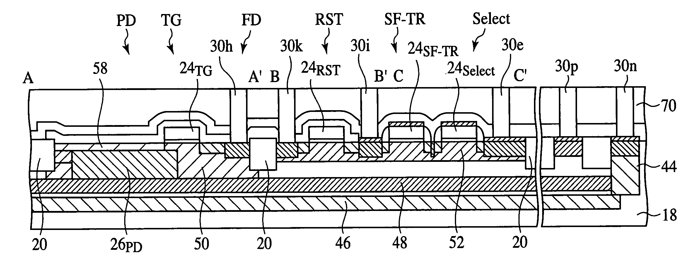
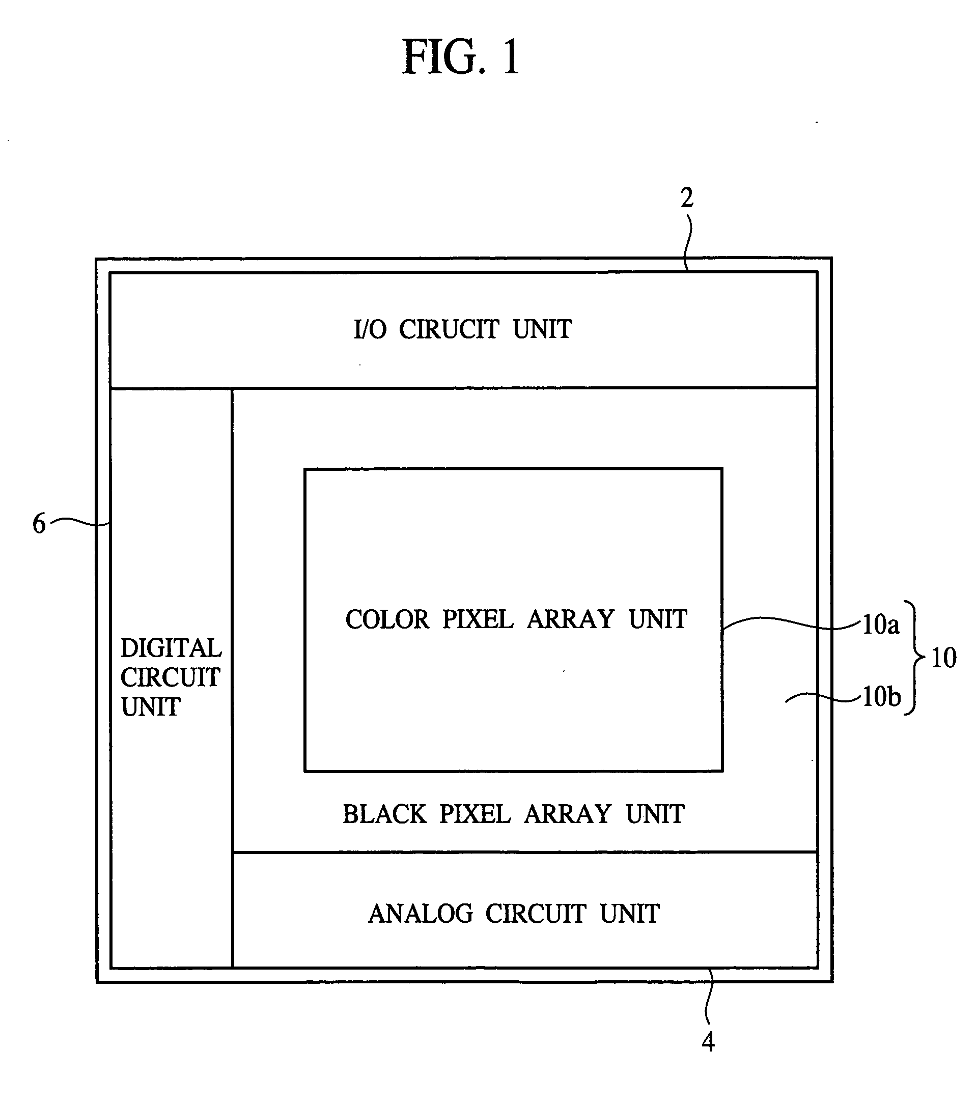
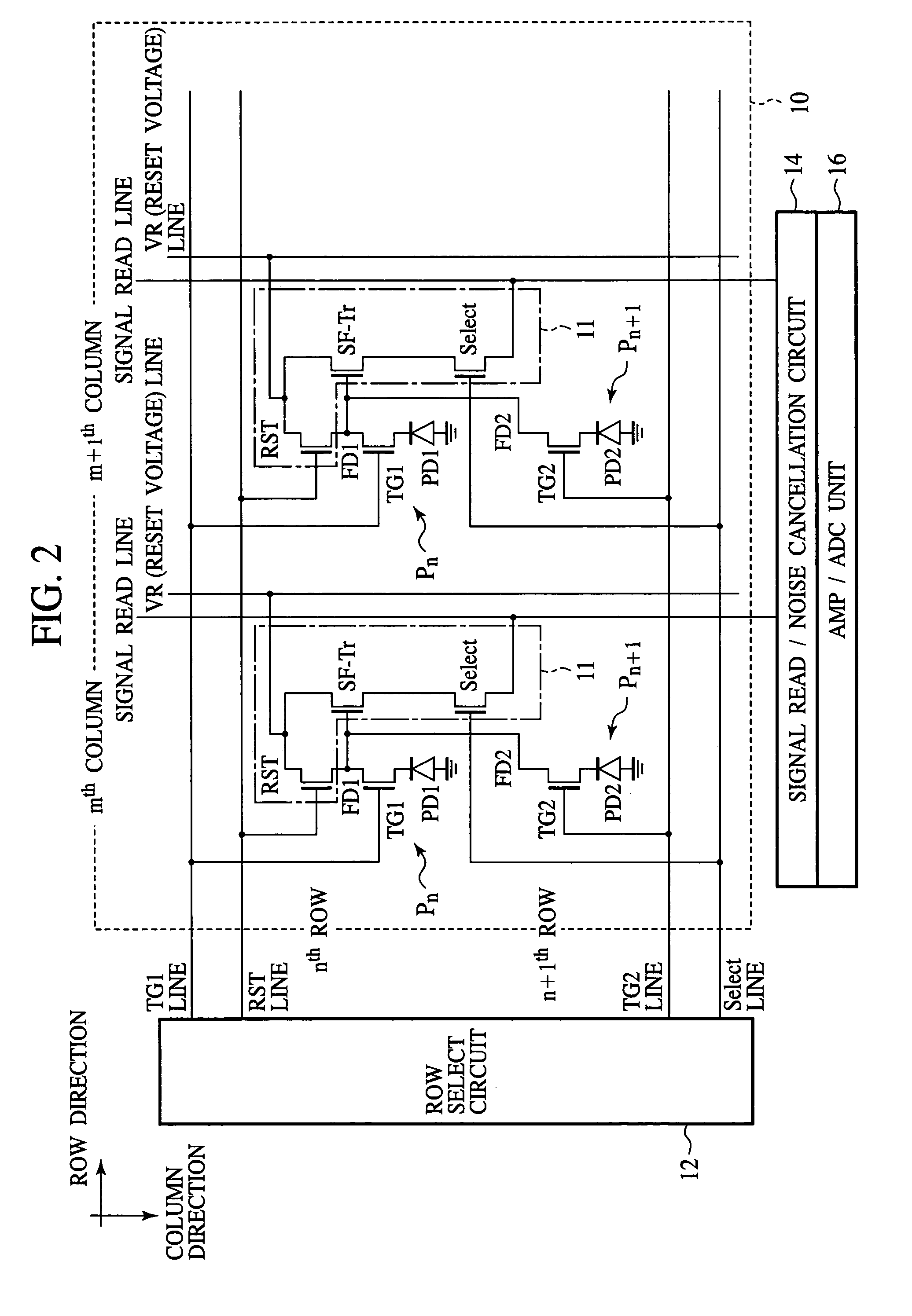
[0040]FIG. 1 is a plan view of a chip image of the solid-state image sensor according to the present embodiment. FIG. 2 is a circuit diagram of the pixel array unit of the solid-state image sensor according to the present embodiment. FIGS. 3-6 are plan views of the solid-state image sensor according to the present embodiment, which show the structure thereof. FIGS. 7A-7B are diagrammatic sectional views of the solid-state image sensor according to the present embodiment, which show the structure thereof. FIG. 8 is a graph of depth-wise changes of the potential of the region for a photodiode formed in of the solid-state image sensor according to the present embodiment. FIGS. 9A and 9B are views of the extension of the depletion layer of the photodiode. FIGS. 10A-17D are sectional views...

second embodiment

A Second Embodiment

[0155] The solid-state image sensor and the method for fabricating the same according to a second embodiment of the present invention will be explained with reference to FIGS. 21A to 23B. The same members of the present embodiment as those of the solid-state image sensor and the method for fabricating the same according to the first embodiment shown in FIGS. 1 to 20 are represented by the same reference numbers not to repeat or to simplify their explanation.

[0156]FIGS. 21A and 21B are diagrammatic sectional views showing a structure and the method for fabricating the same of the solid-state image sensor according to the present embodiment. FIG. 22 is a graph of a depth-wise distribution of boron forming a buried p-type layer. FIGS. 23A and 23B are views explaining distribution differences of the buried p-type layer made by slant ion implantation and by ion implantation normal to the substrate.

[0157] The solid-state image sensor and the method for fabricating the...

third embodiment

A Third Embodiment

[0175] The solid-state image sensor and the method for fabricating the same according to a third embodiment of the present invention will be explained with reference to FIGS. 24A to 25. The same members of the present embodiment as those of the solid-state image sensor and the method for fabricating the same according to the first and the second embodiments shown in FIGS. 1 to 23B are represented by the same reference numbers not to repeat or to simplify their explanation.

[0176]FIGS. 24A and 24B are diagrammatic sectional views of the solid-state image sensor according to the present embodiment, which show a structure thereof. FIG. 25 is a graph of depth-wise changes of the potential in the region for a photodiode to be formed in of the solid-state image sensor according to the present embodiment.

[0177] In the solid-state image sensor according to the first and the second embodiments, the buried n-type layer 26PD is formed under the same conditions for the photod...


PUM


Abstract

A solid-state image sensor comprises a semiconductor substrate of a first conductivity type having a color pixel region and a black pixel region; a first well of the first conductivity type formed in the color pixel region; a second well of the first conductivity type formed in the black pixel region; a third well of a second conductivity type formed, surrounding the second well and isolating the second well from the rest region of the semiconductor substrate; a color pixel formed in the first well in the color pixel region and including a first photodiode and a first read transistor for reading a signal generated by the first photodiode; and a black pixel formed in the second well in the black pixel region and including a second photodiode and a second read transistor for reading a signal generated by the second photodiode. The first well includes a first buried impurity doped layer of the first conductivity type formed in a bottom thereof in a region where the first read transistor is formed. The second well includes a second buried impurity doped layer of the first conductivity type formed in a bottom thereof in a region where the second photodiode is formed and a region where the second read transistor is formed.

Description

CROSS-REFERENCE TO RELATED APPLICATIONS [0001] This application is based upon and claims the benefit of priority from the prior Japanese Patent Application No. 2004-209681, filed on Jul. 16, 2004, the entire contents of which are incorporated herein by reference. BACKGROUND OF THE INVENTION [0002] The present invention relates to a solid-state image sensor formed of CMOS and a method for fabricating the same. [0003] As a solid-state image sensor using semiconductor materials, an image sensor formed of CMOS (CMOS image sensor) is known. [0004] The CMOS image sensor includes a pixel unit shielded from light, which are called a black pixel unit (also optical black unit) in addition to a light receiving unit of color pixel unit. The black pixel unit is for generating a reference value of a pixel signal in a dark state for the prevention of changes of a signal level due to temperature changes, etc. Accordingly, it is preferable that the black pixel unit is formed isolatable from noises o...

Claims


Application Information

Patent Timeline
IPC IPC(8): H01L21/00H01L31/113H01L27/146H04N5/335H04N5/361H04N5/369H04N5/374
CPCH01L27/14603H01L27/14609H01L27/14623H01L27/14641H01L27/14645H01L27/14689H01L27/1463H01L27/14H01L27/146H01L31/10
Inventor OHKAWA, NARUMI
Owner FUJITSU SEMICON LTD
Why Eureka
Try Eureka