High frequency MOS transistor, method of forming the same, and method of manufacturing a semiconductor device including the same

a technology of high-frequency metal oxide semiconductors and transistors, which is applied in the direction of semiconductor devices, electrical equipment, basic electric elements, etc., can solve the problems of affecting the performance of ldmos transistors, fatal signal loss through a channel in real transistors, and breakdown voltages that are generally incompatible with transistor on-resistance, so as to improve transistor electrical characteristics, reduce transistor on-resistance, and reduce the effect of transistor capacitance between the gate structure and drain

Inactive Publication Date: 2006-01-19
SAMSUNG ELECTRONICS CO LTD
View PDF3 Cites 24 Cited by
  • Summary
  • Abstract
  • Description
  • Claims
  • Application Information

AI Technical Summary

Benefits of technology

[0027] In another aspect, the present invention is directed to a method of manufacturing a semiconductor device. A semiconductor substrate on which a semiconductor layer is formed is provided, and a surface of the substrate is divided into a lateral double-diffused metal oxidation of silicon (LDMOS) region in which an LDMOS transistor is formed, a PMOS region in which a P-type transistor is formed and an NMOS region in which an N-type transistor is formed. N-type impurities are partially implanted into the LDMOS region and the PMOS region at a second concentration, so that a buffer N-well is formed on a first portion of the LDMOS region and the N-well of the P-type transistor is formed on the PMOS region. A P-well of the N-type transistor is formed on the NMOS region by partially implanting P-type impurities into the NMOS region. First, second and third gate structures are formed on the LDMOS region spaced apart from the buffer N-well, on the NMOS region and the PMOS region, respectively. A lightly doped drain (LDD) is formed on the LDMOS region by implanting N-type impurities into the LDMOS region between the first gate structure and the buffer N-well, and a lightly doped N-type area is formed on the NMOS region around the second gate structure by implanting the N-type impurities into the NMOS region at a third concentration lower than the second concentration. A source and a drain of the LDMOS transistor are formed at surface portions of the LDMOS region and source and drain regions of the N-type transistor are formed at surface portions of the NMOS region by partially implanting N-type impurities into the LDMOS and NMOS regions of the substrate at a first concentration higher than the second concentration. The source of the LDMOS transistor is formed adjacent to the first gate structure on a second portion of the LDMOS region, opposite to the first portion of the LDMOS region with respect to the first structure. The drain of the LDMOS transistor is formed on a substrate corresponding to the buffer N-well, and the source and drain of the NMOS transistor are formed adjacent to the second gate structure and opposite to each other with respect to the second gate structure. A source and a drain of the P-type transistor are formed at surface portions of the PMOS region by partially implanting P-type impurities into the PMOS region adjacent to the third gate structure and opposite to each other with respect to the third gate structure. According to the present invention, the buffer well surrounds the drain of the transistor, so that an on-resistance of the transistor is decreased and electrical characteristics of the transistor are improved. In addition, the buffer well is not overlapped with the gate structure of the transistor, so that a capacitance between the gate structure and the drain is not increased despite the buffer well. Therefore, frequency characteristics of the transistor are not deteriorated due to the buffer well.

Problems solved by technology

In particular, the breakdown voltage and the on-resistance greatly affect the performance of the LDMOS transistor when the LDMOS transistor is operated at a high frequency.
As a result, an excessively low off-resistance causes a leakage current, and an excessively high on-resistance leads to a fatal signal loss through a channel in real transistors.
However, the breakdown voltage is generally incompatible with the on-resistance of a transistor.
A high breakdown voltage necessarily causes a high on-resistance of a transistor, and a low on-resistance of a transistor necessarily requires a low breakdown voltage.
When the breakdown voltage is low, a capacitance between a gate and a drain of a transistor is increased, so that an operation failure frequently occurs in a high frequency transistor.

Method used


Image

  • High frequency MOS transistor, method of forming the same, and method of manufacturing a semiconductor device including the same
  • High frequency MOS transistor, method of forming the same, and method of manufacturing a semiconductor device including the same
  • High frequency MOS transistor, method of forming the same, and method of manufacturing a semiconductor device including the same

Examples


embodiment 1

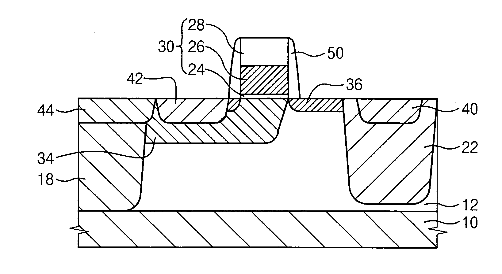
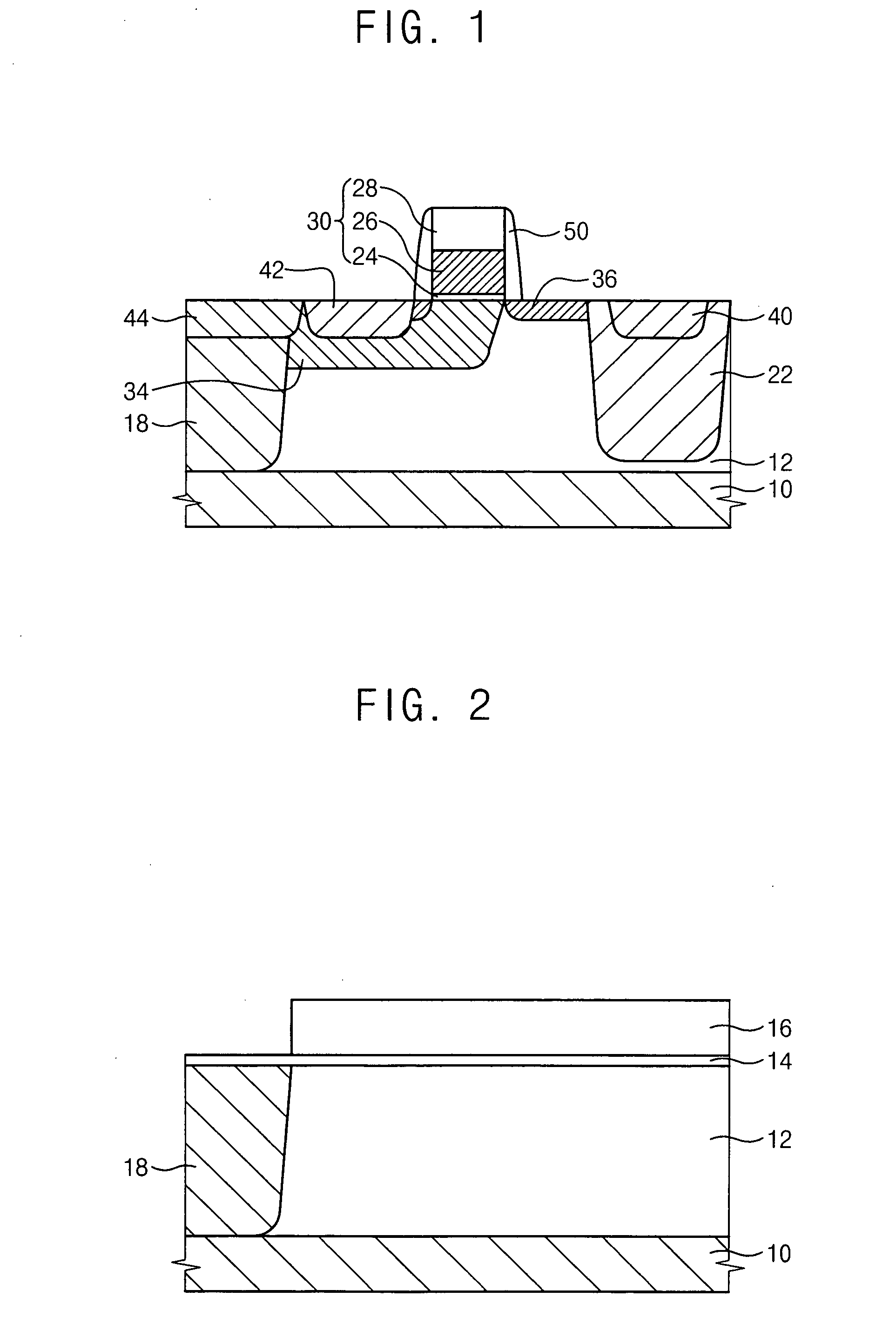
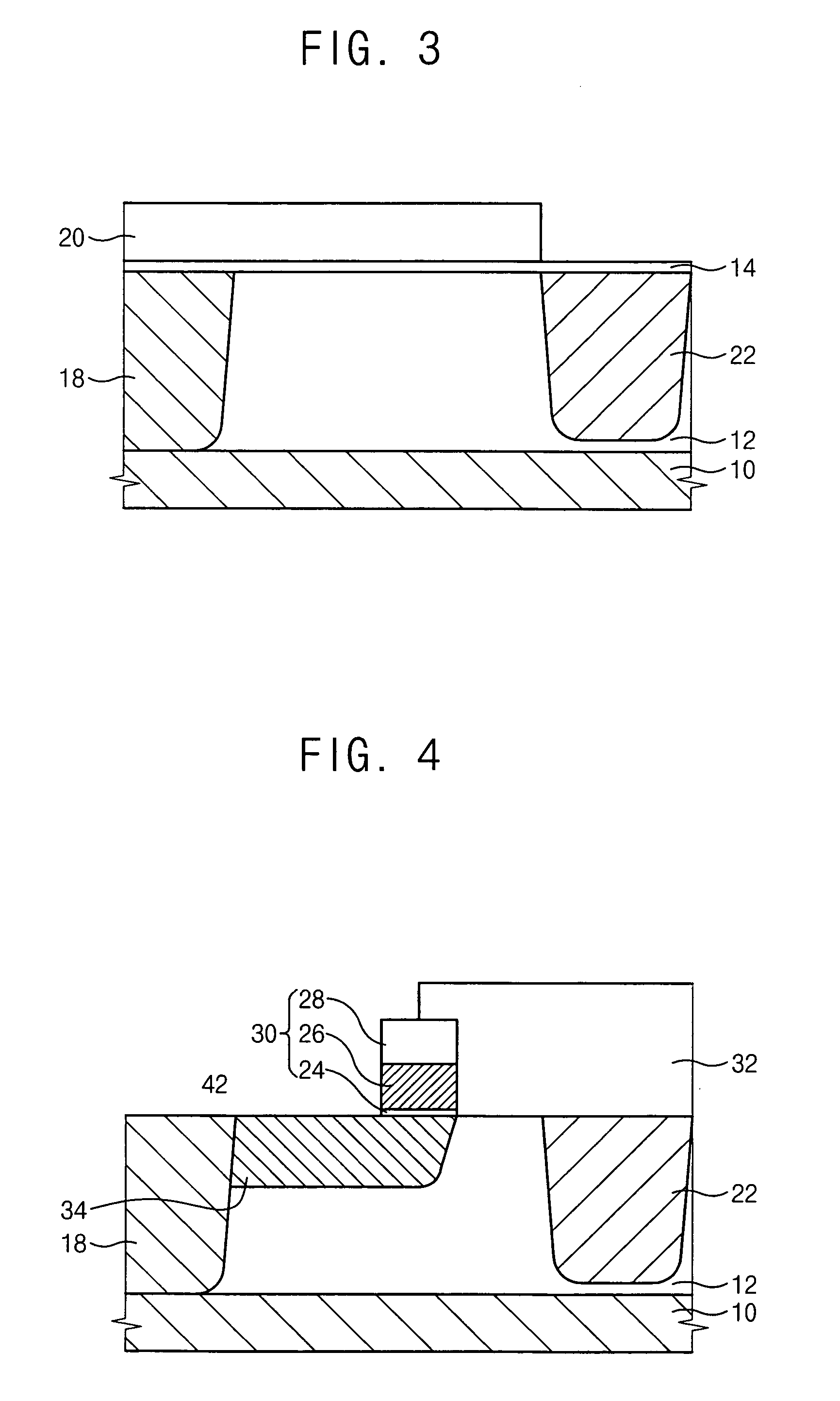
[0043]FIG. 1 is a cross sectional view illustrating a high frequency LDMOS transistor in accordance with a first exemplary embodiment of the present invention.

[0044] Referring to FIG. 1, a semiconductor layer 12 is formed through an epitaxial process on a semiconductor substrate 10 heavily doped with P-type impurities. In the present embodiment, the semiconductor layer 12 on the semiconductor substrate 10 is formed to a thickness in a range from about 1 μm to about 10 μm, and is doped with P-type impurities at a relatively lower concentration than the semiconductor substrate 10.

[0045] A gate structure 30 is formed on the semiconductor layer 12. The gate structure 30 includes a gate insulation pattern 24 having a uniform thickness, a gate electrode pattern 26 and a hard mask pattern 28 that are sequentially stacked on the semiconductor layer 12 in the order named above. A spacer 50 is formed on a side surface of the gate structure 30.

[0046] N-type impurities are implanted at a sur...

embodiment 2

[0067] FIGS. 7 to 11 are cross sectional views illustrating processing steps for a method of manufacturing a semiconductor device having both a high frequency LDMOS transistor and a CMOS transistor according to a second exemplary embodiment of the present invention.

[0068] Referring to FIG. 7, a semiconductor layer 102 is formed to a thickness of about 1 μm to about 10 μm on a semiconductor substrate 100 heavily doped with P-type impurities through an epitaxial process, and the P-type impurities are implanted through a surface of the semiconductor layer 102 more lightly than the substrate 100 in-situ with the above epitaxial process or in an additional process different from the epitaxial process. In the present embodiment, the semiconductor layer 102 is divided into three distinct regions: an LDMOS region in which the high frequency LDMOS transistor is to be formed, an NMOS region in which an NMOS transistor of a CMOS transistor is formed and a PMOS region in which a PMOS transisto...


PUM


Abstract

In a high frequency LDMOS transistor, a gate structure is formed on a substrate. A drain, doped with first type impurities at a first concentration, is formed on the substrate spaced apart from the gate structure. A buffer well, doped with the first type impurities at a second concentration lower than the first concentration, surrounds side and lower portions of the drain. A lightly doped drain, doped with the first type impurities at a third concentration lower than the second concentration, is formed between the buffer well and the gate structure. A source, doped with the first type impurities at the first concentration, is formed on the substrate adjacent to the gate structure and opposite to the drain with respect to the gate structure. Accordingly, an on-resistance decreases while a breakdown voltage increases in the LDMOS transistor without increasing a capacitance between the gate structure and the drain.

Description

CROSS REFERENCE TO RELATED APPLICATION [0001] This application claims priority under 35 USC § 119 to Korean Patent Application No. 2004-55061, filed on Jul. 15, 2004, the contents of which are herein incorporated by reference in their entirety for all purposes. BACKGROUND OF THE INVENTION [0002] 1. Field of the Invention [0003] The present invention relates to a high frequency metal oxide semiconductor (MOS) transistor, a method of forming the same and a method of manufacturing a semiconductor device including the same. More particularly, the present invention relates to a high frequency lateral double-diffused (LD) MOS transistor, a method of forming the same, and a method of manufacturing a semiconductor device having the LDMOS transistor. [0004] 2. Description of the Related Art [0005] Semiconductor transistors can generally be classified as a bipolar junction transistor (BJT) and a field effect transistor (FET) in accordance with the type of charge carrier thereof. [0006] While ...

Claims


Application Information

Patent Timeline
Patent Type & Authority Applications(United States)
IPC IPC(8): H01L29/78H01L21/8238H01L21/336
CPCH01L21/823807H01L21/823814H01L29/7835H01L29/0847H01L29/66659H01L27/0922H01L21/2253H01L27/0928
Inventor LEE, SUN-HAK
Owner SAMSUNG ELECTRONICS CO LTD
Why Eureka
Try Eureka