Ferroelectric random access memory capacitor and method for manufacturing the same

a random access memory and capacitor technology, applied in the field of semiconductor devices, can solve the problems of deterioration of the ferroelectric property of the feram capacitor, several shortcomings of the conventional method for manufacturing the feram capacitor, etc., and achieve the effect of enhancing the ferroelectric property and preventing the cracking of the ferroelectric layer

Active Publication Date: 2006-01-19
SK HYNIX INC
View PDF6 Cites 39 Cited by
  • Summary
  • Abstract
  • Description
  • Claims
  • Application Information

AI Technical Summary

Benefits of technology

[0018] It is, therefore, an object of the present invention to provide a ferroelectric random access memory (FeRAM) capacitor having a merged top electrode plate line (MTP) structure therein by employing a one-step etching for forming a vertical capacitor stack, thereby enhancing a ferroelectric property and preventing a crack in the ferroelectric layer.
[0019] It is another object of the present invention to provide a method for manufacturing the FeRAM device with the MTP structure by employing a one-step etching for forming a vertical capacitor stack, thereby enhancing a ferroelectric property and preventing a crack in the ferroelectric layer.

Problems solved by technology

However, the conventional method for manufacturing the FeRAM capacitor as aforementioned suffers from several shortcomings.
In the long run, a ferroelectric property of the FeRAM capacitor becomes deteriorated.

Method used


Image

  • Ferroelectric random access memory capacitor and method for manufacturing the same
  • Ferroelectric random access memory capacitor and method for manufacturing the same
  • Ferroelectric random access memory capacitor and method for manufacturing the same

Examples


Embodiment Construction

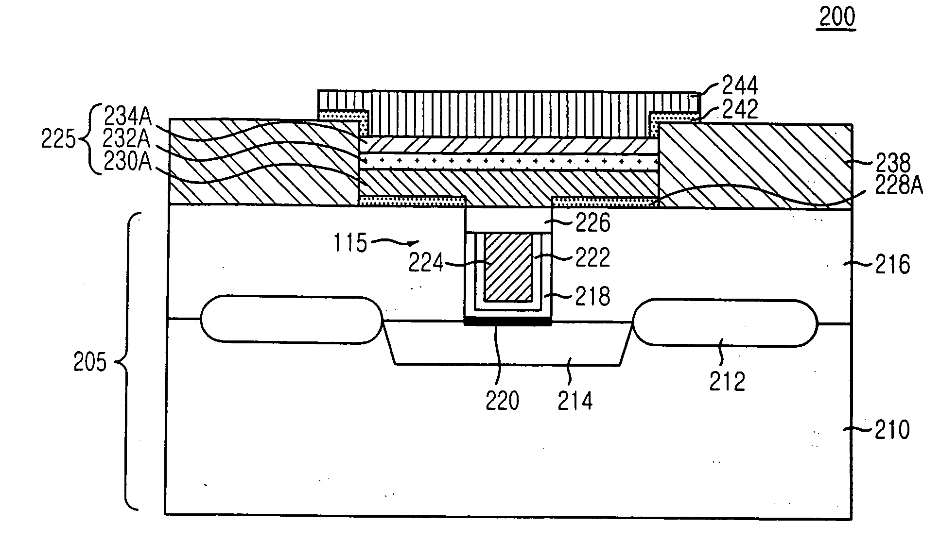
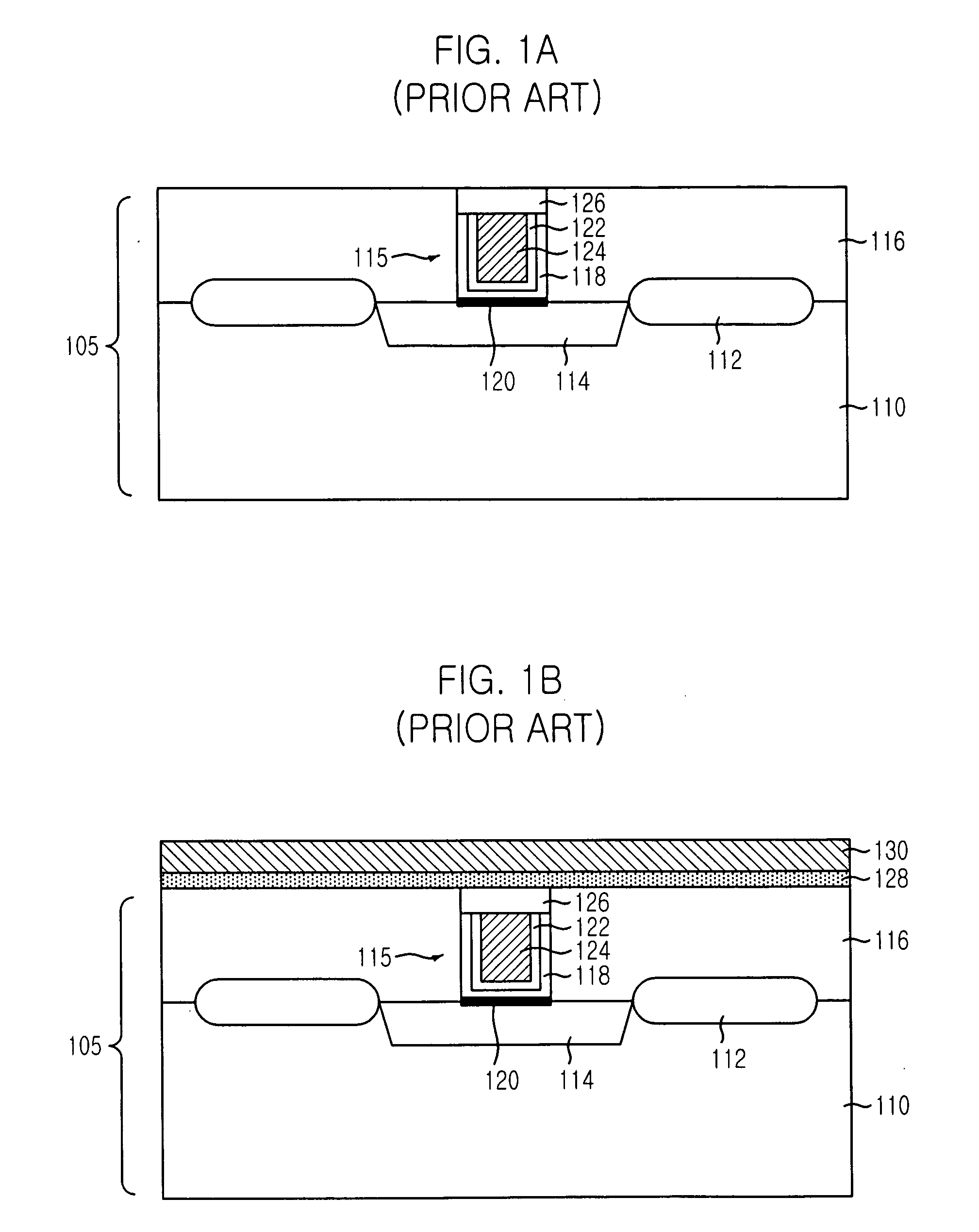
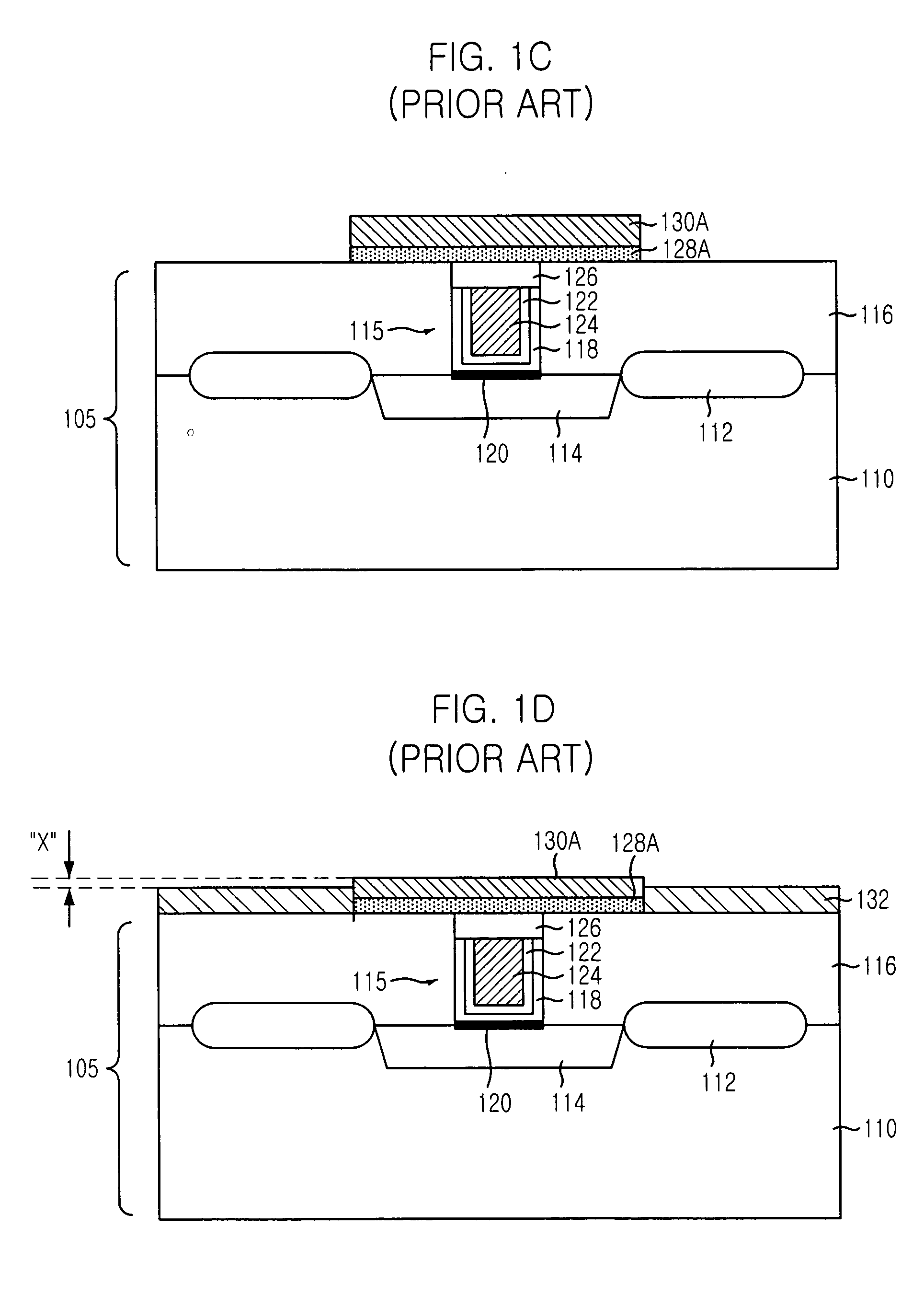
[0028] There are provided in FIG. 2, FIGS. 3A to 3F, FIG. 4 and FIG. 5 cross sectional views and a plane view setting forth a ferroelectric random access memory (FeRAM) capacitor and a method for manufacturing the same in accordance with a preferred embodiment of the present invention. It should be noted that like parts appearing in FIG. 2, FIGS. 3A to 3F, FIG. 4 and FIG. 5 are represented by like reference numerals.

[0029] Referring to FIG. 2, there is shown a cross sectional view illustrating an inventive FeRAM capacitor 200 with a merged top electrode plate line (MTP) structure including an active matrix 205, a capacitor stack 225, a second interlayer dielectric (ILD) 238 and a plate line 244. The active matrix 205 includes a semiconductor substrate 210 having field oxide (FOX) regions 212 and a source / drain region 214, a first ILD 216 formed on the semiconductor substrate 210 and a storage node contact 215 achieved after patterning the first ILD 216 into a predetermined configur...


PUM


Abstract

The method for manufacturing an FeRAM capacitor with a merged top electrode plate line (MTP) structure is employed to prevent a detrimental impact on the FeRAM and to secure a reliable FeRAM device. The method includes steps of: preparing an active matrix obtained by a predetermined process; forming a first conductive layer, a dielectric layer and a second conductive layer on the active matrix in sequence; forming a hard mask on the second conductive layer; patterning the second conductive layer, the dielectric layer and the first conductive layer by using the hard mask, thereby forming a vertical capacitor stack, a width of the capacitor stack being larger than that of the storage node contact; forming a second ILD embracing the capacitor stack; planarizing the second ILD till the top face of the hard mask is exposed; removing the hard mask to form an opening above the top electrode; and forming a plate line of which a width is larger than that of the capacitor stack.

Description

FIELD OF THE INVENTION [0001] The present invention relates to a semiconductor device and a method for manufacturing the same; and, more particularly, to a ferroelectric random access memory (FeRAM) capacitor having a merged top electrode plate line (MTP) structure therein and a method for manufacturing the same. DESCRIPTION OF THE PRIOR ART [0002] With the recent progress of film deposition techniques, researches for a nonvolatile memory cell using a ferroelectric thin film have increasingly been developed. This nonvolatile memory cell is a high-speed rewritable nonvolatile characteristic utilizing high-speed polarization / inversion and residual polarization of a ferroelectric capacitor thin film. [0003] Therefore, a ferroelectric random access memory (FeRAM) where a ferroelectric material such as strontium bismuth tantalate (SBT) and lead zirconium titanate (PZT) is increasingly used for the capacitor thin film in place of a conventional silicon oxide film or a silicon nitride film...

Claims


Application Information

Patent Timeline
Patent Type & Authority Applications(United States)
IPC IPC(8): H01L21/00H01L21/02H01L21/768H01L27/105H01L21/822H01L21/8239H01L21/8246H01L27/115H01L29/76H01L29/94
CPCH01L21/76895H01L27/11502H01L28/75H01L28/57H01L27/11507H10B53/30H10B53/00H01L27/105
Inventor KWEON, SOON-YONG
Owner SK HYNIX INC
Why Eureka
Try Eureka