
Image sensor with light guides
a technology of image sensor and light guide, which is applied in the direction of optical elements, radio frequency control devices, instruments, etc., can solve the problems of black and white sensor image resolution degradation, color sensor limitation, and difficult material selection, so as to reduce crosstalk
- Summary
- Abstract
- Description
- Claims
- Application Information
AI Technical Summary
Benefits of technology
Problems solved by technology
Method used
Image

Examples
Embodiment Construction
[0028] The present invention provides an image sensor device and fabrication method thereof. The image sensor device is very suitable for a solid state image sensor, such as a CCD (charge-coupled device) or a CMOS (complementary metal-oxide semiconductor) imager. In order to simplify the illustration, a representative photodiode array serving as a photosensor array is illustrated in the preferred embodiment of the present invention; the peripheral regions of the image sensor device are not illustrated.
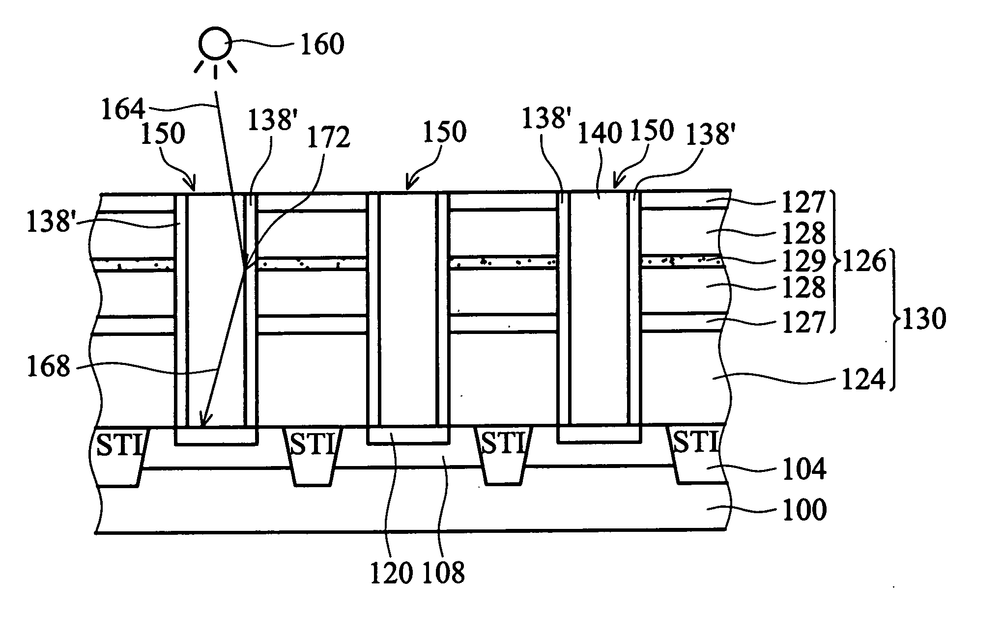
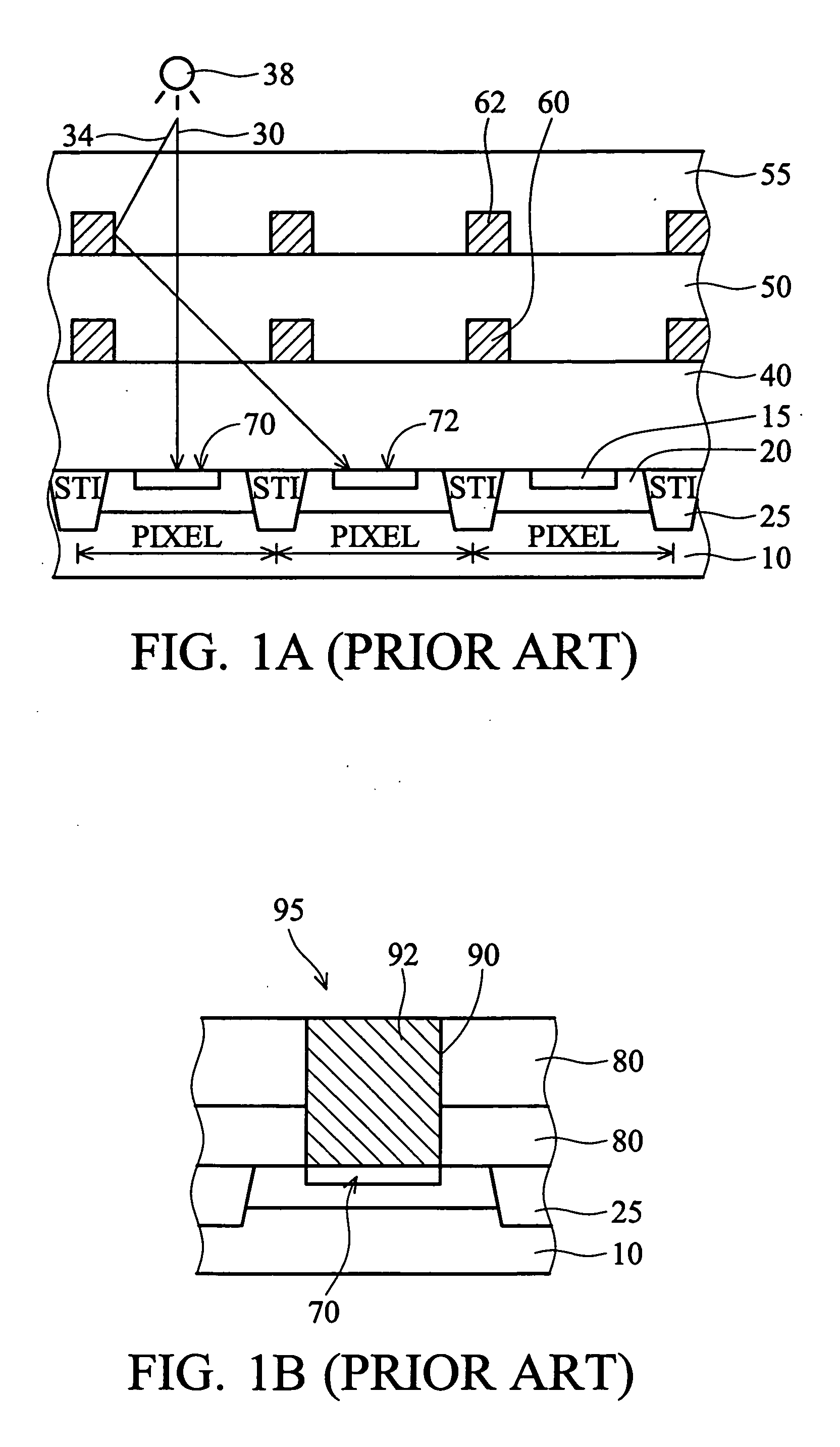
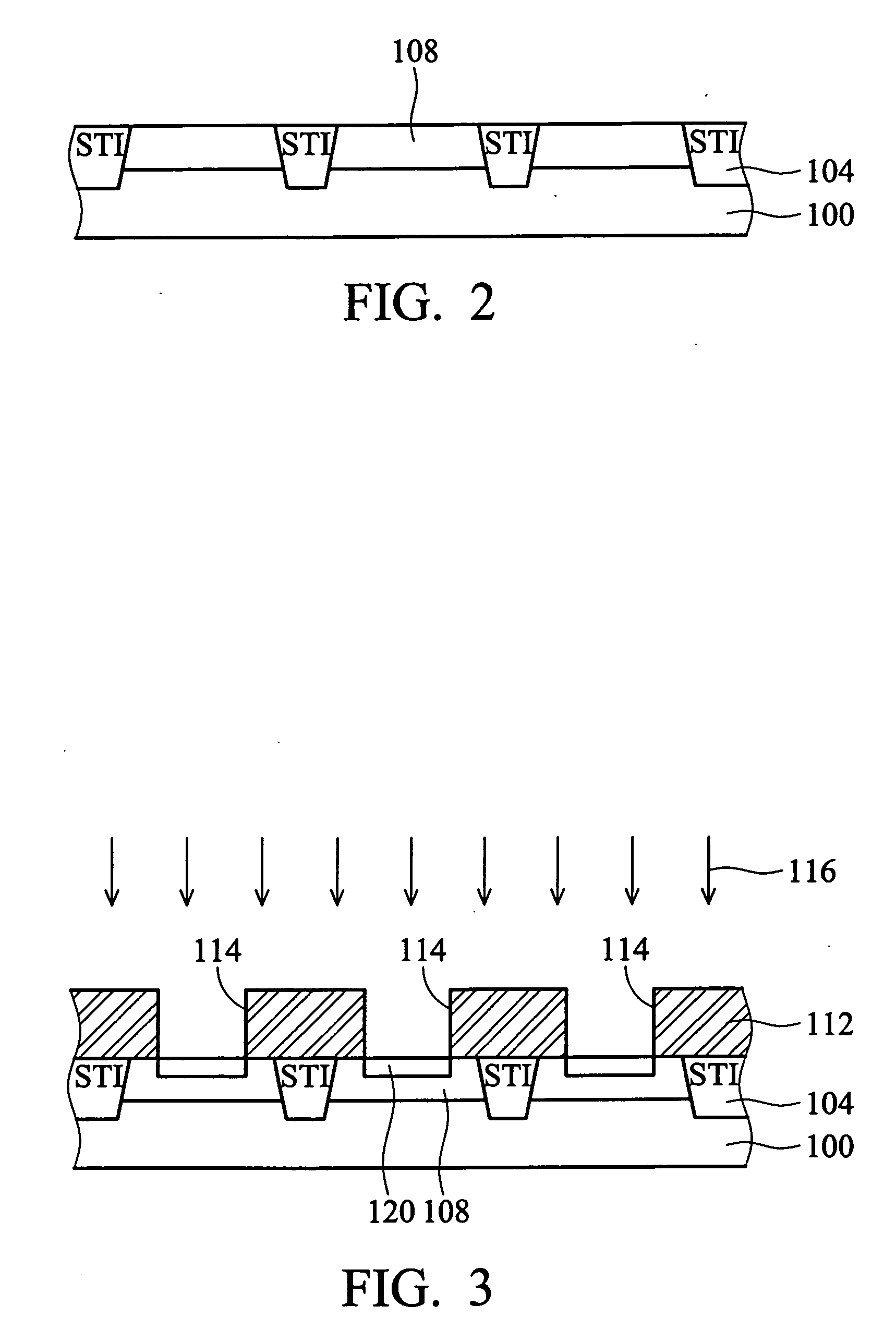
[0029] FIGS. 2˜9 illustrate a process of manufacturing a modified image sensor device of the present invention. FIG. 10 illustrates the improved performance of the preferred embodiment of the present invention. Several important features of the present invention are shown therein and discussed below. The embodiments of the present invention are applied to the formation of a unique, image sensor array comprising a plurality of photodiodes (i.e. photosensors) formed in a semiconductor s...
PUM
 Abstract
Description
Claims
Application Information