Method for manufacturing soi wafer

a technology of silicon on insulator and soi, which is applied in the direction of basic electric elements, electrical apparatus, semiconductor devices, etc., can solve the problems of difficult discrimination, line defect, and problem of problem of line-shaped defect present on the surface of a bond wafer, and achieves stable annihilation, easy annihilation, and reduced generation of voids

Inactive Publication Date: 2006-01-19
SHIN-ETSU HANDOTAI CO LTD
View PDF2 Cites 27 Cited by
  • Summary
  • Abstract
  • Description
  • Claims
  • Application Information

AI Technical Summary

Benefits of technology

[0029] As conditions for the high temperature heat treatment, wafers are heat treated at a high temperature of 1100° C. or higher. The temperature is especially preferably in the range of 1100° C. to 1350° C. If the temperature is at 1000° C., there is a case where a line defect is not sufficiently annihilated, while the temperature is 1100° C. or higher, a line defect can be stably annihilated. The upper limit of the temperature is not specifically limited and a temperature of the melting point or lower can be adopted, whereas a temperature closer to the melting point causes easily other problems including generation of many slips; therefore, treatment at a temperature of 1350° C. or lower is preferable. A heat treatment ti

Problems solved by technology

Especially, a line-shaped defect present on a surface of a bond wafer has been found to be problematic.
This line defect is, however, difficult in discrimination from COP, and it

Method used


Image

  • Method for manufacturing soi wafer
  • Method for manufacturing soi wafer
  • Method for manufacturing soi wafer

Examples


experimental example 1

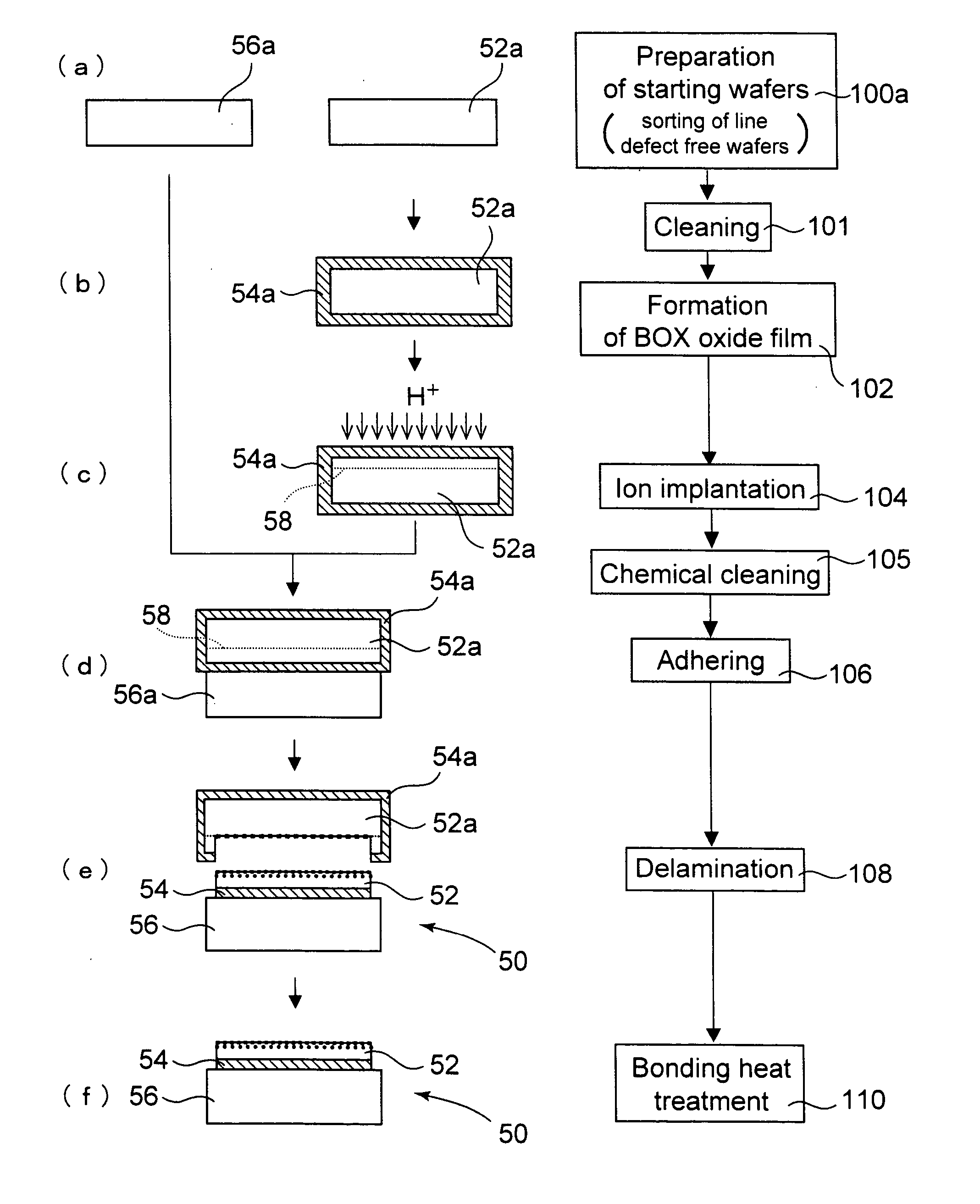
[0054] Description will be given of a conventional method for an SOI wafer below with reference to FIGS. 3 to 5 while schematically showing an influence of a line defect. At first, as a base wafer 56a and a bond wafer 52a, there were prepared p-type mirror-polished silicon wafers each having a diameter of 300 mm, a orientation and a resistivity of 10 Ω·cm manufactured from an ingot grown by a CZ method [FIG. 5(a), step 100]. The starting wafers were wafers on a surface of each of which about 100 line defects were observed. The sizes of the line defects each were 0.5 μm or more in diameter. The line defects were, as shown in FIG. 3, usually observed as a size of the order in the range of from 2 to 3 μm.

[0055] Observation of a line defect was conducted using a laser microscope with a confocal optical system. The laser microscope with a confocal optical system is one manufactured by Lasertech Co. with a trade name of MAGICS.

[0056] With the wafers described above, there was formed an...

example 1

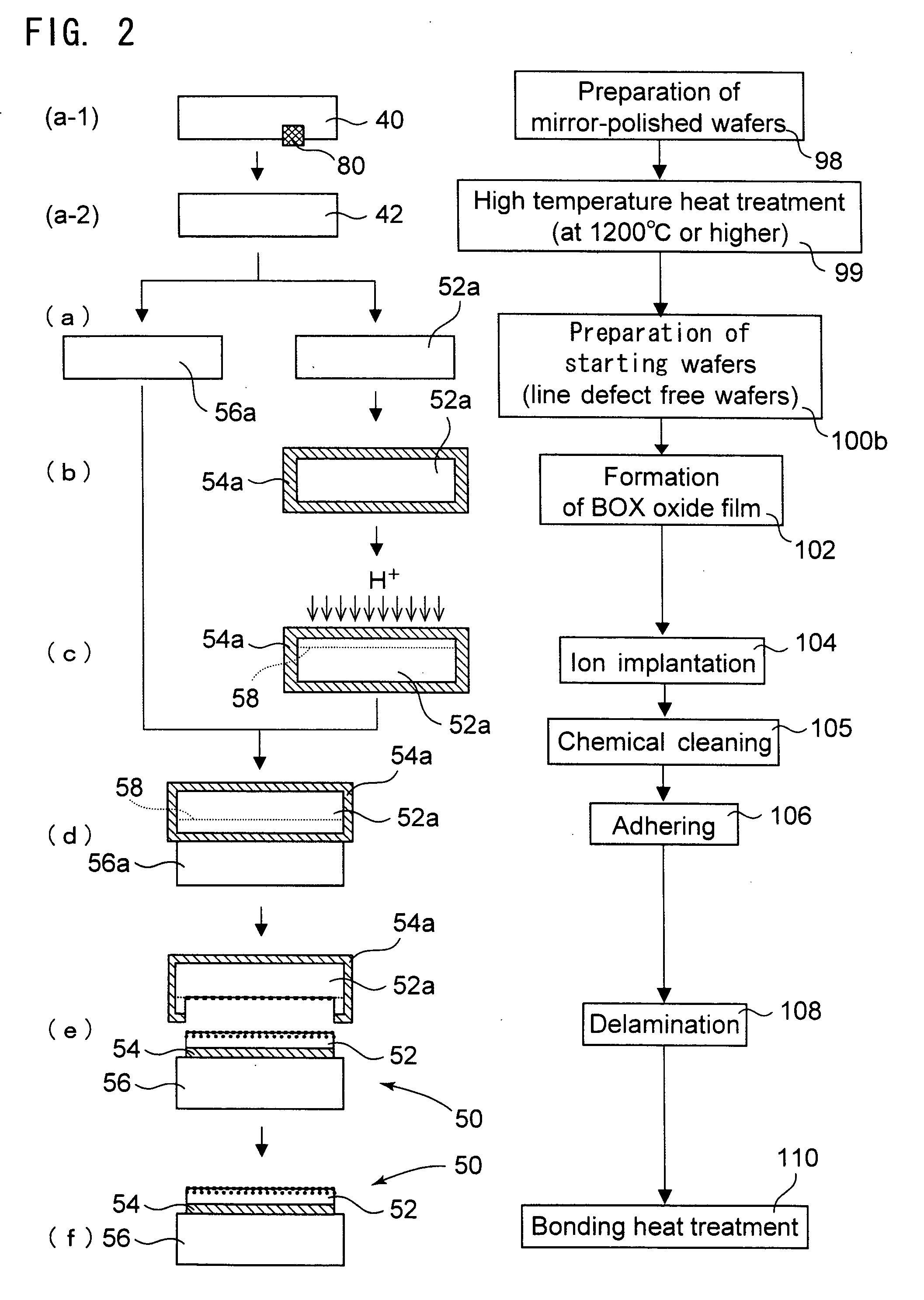
[0061] An SOI wafer 50 was manufactured according to a manufacturing process of a method of the present invention shown in FIG. 2. At first, there were prepared p-type mirror-polished silicon wafers each having a diameter of 200 mm, a orientation and a resistivity of 10 Ω·cm manufactured from an ingot grown by a CZ method [FIG. 2(a-1), step 98].

[0062] The starting wafers were first subjected to high temperature heat treatment [FIG. 2(a-2), step 99]. The high temperature heat treatment was carried out with a vertical heater heating type heat treatment apparatus (a batch furnace) in a 100% argon atmosphere at 1200° C. for 1 hr. In the heat treatment, a temperature rise rate up to 1000° C. was 5° C. / min. and thereafter the rate up to 1200° C. was 2° C. / min., while a temperature fall rate was 2° C. / min.

[0063] Each of the wafer surfaces was inspected on a line defect using a laser microscope with a confocal optical system and absence of a line defect was confirmed on all the wafers. T...


PUM


Abstract

The present invention provides a manufacturing method for an SOI wafer with a high productivity in which generation of a void is suppressed in manufacturing the SOI wafer. In a manufacturing method for an SOI wafer of the present invention in which two starting wafers are prepared, an insulating layer is formed on at least one of the two starting wafers and the one wafer is adhered to the other wafer without using an adhesive agent, the starting wafers each with no line defect on a surface thereof are used. In a manufacturing method for an SOI wafer of the present invention in which two starting wafers are prepared, an insulating layer is formed on at least one of the two starting wafers and the one wafer is adhered to the other wafer without using an adhesive agent, the starting wafers are subjected to a high temperature heat treatment in advance.

Description

TECHNICAL FIELD [0001] The present invention relates to a method for manufacturing an SOI (Silicon on Insulator) wafer constituted of an SOI layer, an insulating layer and a support substrate, and particularly, to a method for manufacturing an SOI wafer by means of a bonding method (an adhering method). BACKGROUND ART [0002] In recent years, an integration level in an integrated circuit has greatly increased, which has been accompanied by stricter required conditions imposed on a manufacturing precision such as flatness or smoothness of a mirror-polished wafer surface. In addition, in order to achieve an integrated circuit higher in performance, reliability and product yield, not only a higher mechanical precision, but also better electric characteristics have been required. Especially, an SOI wafer, which is an ideal dielectric isolation substrate, has been used in applications to high frequency and high-speed devices mainly related to mobile communication equipment and medical equ...

Claims


Application Information

Patent Timeline
IPC IPC(8): H01L21/84H01L21/02H01L21/306H01L21/762H01L27/12
CPCH01L21/76254H01L21/02043
Inventor ICHIKAWA, MASASHIKOBAYASHI, TAKESHIIWABUCHI, MIHO
Owner SHIN-ETSU HANDOTAI CO LTD
Why Eureka
Try Eureka