Charged particle beam drawing equipment, method of adjusting aperture mask, and method of manufacturing semiconductor device

Inactive Publication Date: 2006-01-26
KK TOSHIBA
View PDF2 Cites 5 Cited by
  • Summary
  • Abstract
  • Description
  • Claims
  • Application Information

AI Technical Summary

Benefits of technology

[0008] According to an aspect of the present invention, there is provided a charged particle beam drawing equipment comprising: a charged particle beam source configured to emit a charged particle beam; a first shaping aperture mask provided below the charged particle beam source and comprising a plurality of opening portions which include a first opening portion for rotation adjustment; a second shaping aperture mask provided below the first shaping aperture mask and comprising a plurality of opening portions which include a second opening portion for rotation adjustment; a detection section configured to detect an intensity distribution of charged particle beam, the intensity distribution being in a plane substantially parallel to the second shaping aperture mask, the charged particle beam being emitted from the charged particle beam source and passing through the first and second opening portions for rotation adjustment; a rotation angle control section configured to control a relative rotation angle between the fi

Problems solved by technology

However, it is difficult to form the edge of the opening portion of each aperture mask with high precision.
Therefore, the conventional aperture mask adjusting method cannot be simply used because it requires a long time interval or a precisely formed edge.

Method used


Image

  • Charged particle beam drawing equipment, method of adjusting aperture mask, and method of manufacturing semiconductor device
  • Charged particle beam drawing equipment, method of adjusting aperture mask, and method of manufacturing semiconductor device
  • Charged particle beam drawing equipment, method of adjusting aperture mask, and method of manufacturing semiconductor device

Examples


Embodiment Construction

[0017] Hereinafter, embodiments of the present invention will be described with reference to the accompanying drawings.

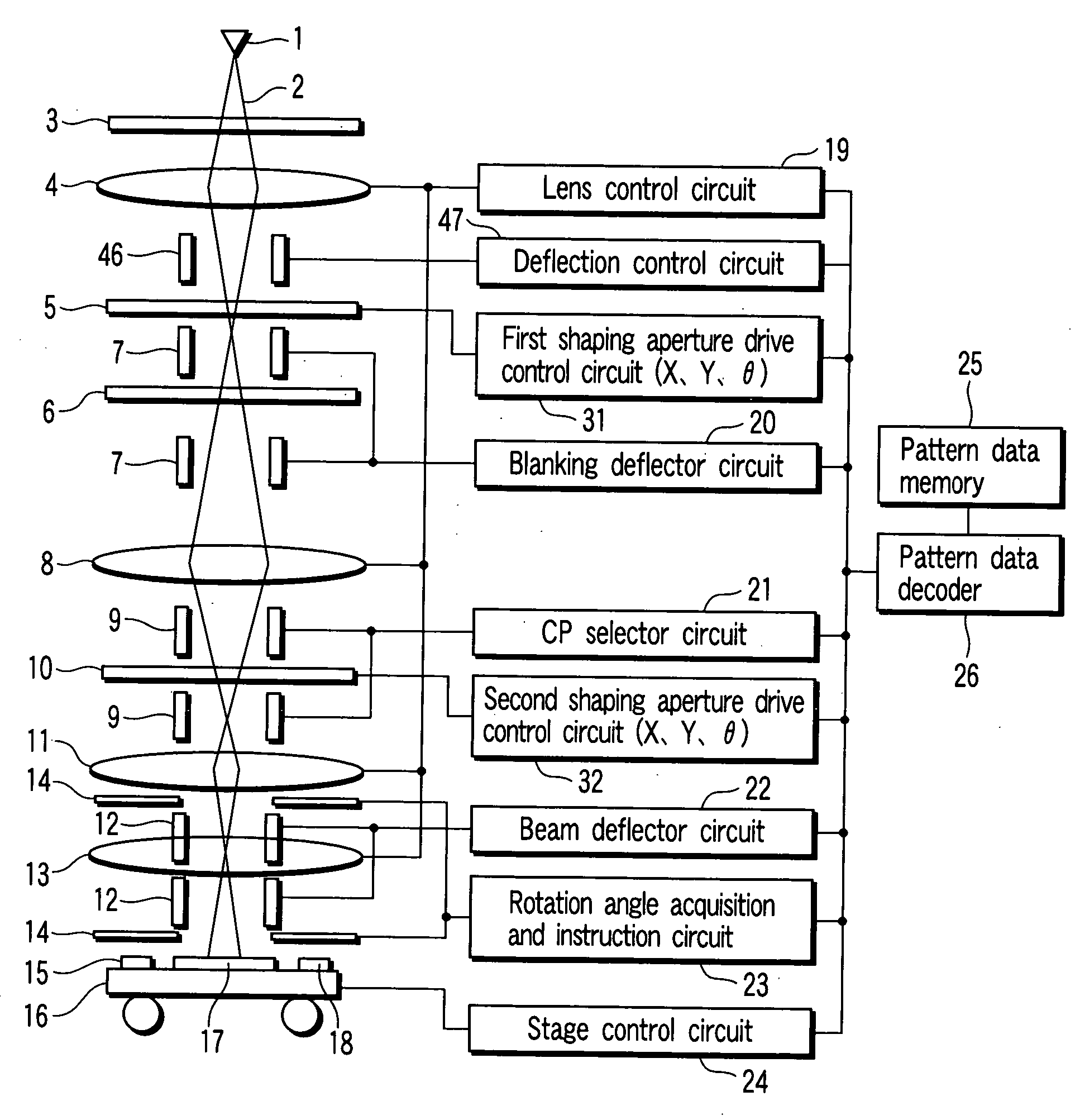
[0018]FIG. 1 is a diagram schematically depicting a general configuration of a charged particle beam drawing equipment according to an embodiment of the present invention.

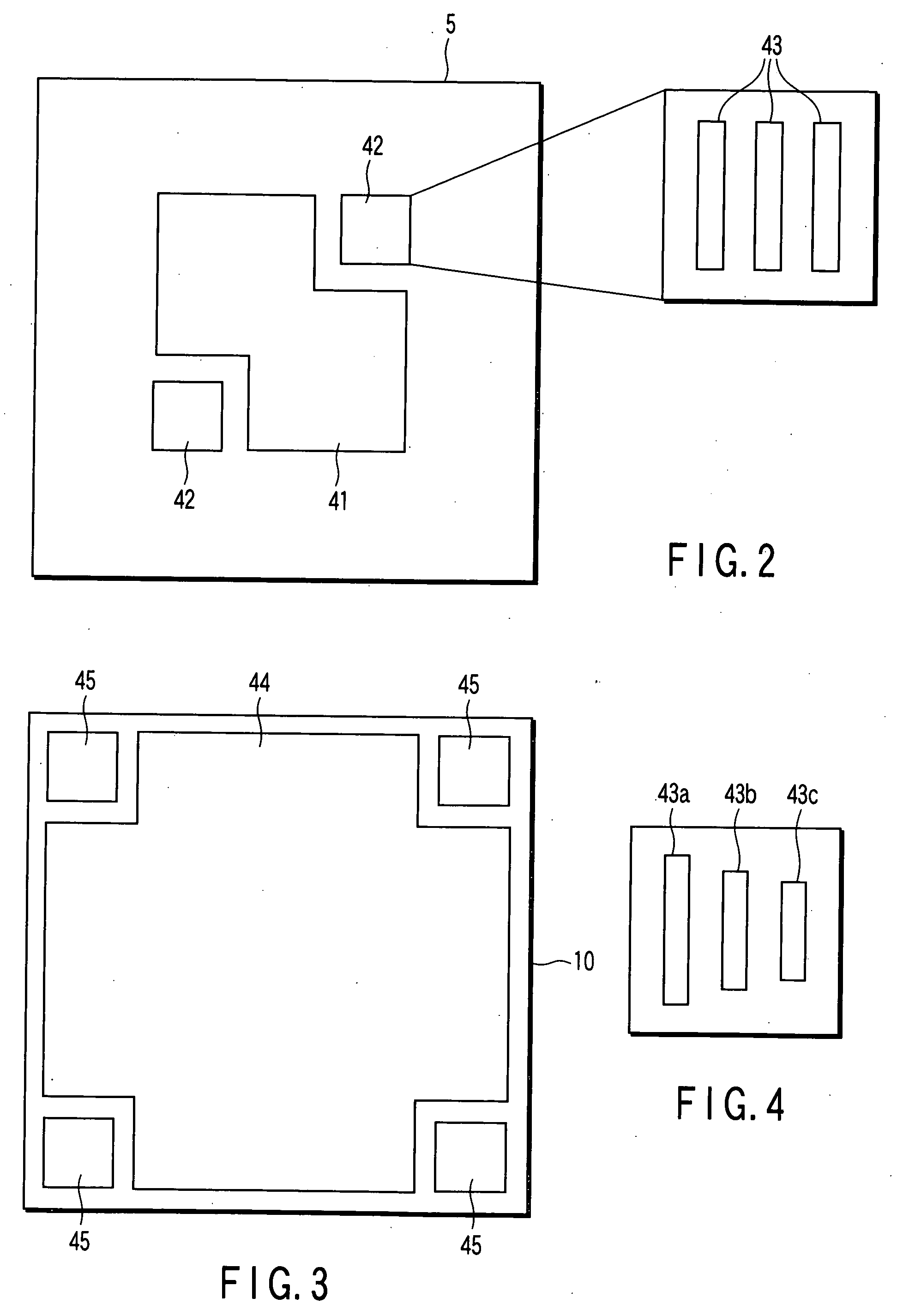
[0019] The charged particle beam drawing equipment according to the present embodiment primarily comprises an electron gun 1, the first shaping aperture mask 5, the second shaping aperture mask 10, a detector 14, the first shaping aperture drive control circuit 31, and a rotation angle acquisition / instruction circuit 23. The electron gun 1 emits a charged particle beam 2. The first shaping aperture mask 5 is provided below the electron gun 1, and has a plurality of opening portions which include the first opening portion for rotation adjustment. The second shaping aperture mask 10 is provided below the first shaping aperture mask 5, and has a plurality of opening portions which include the second...


PUM


Abstract

A charged particle beam drawing equipment includes charged particle beam source, first and second shaping aperture masks with first and second opening portions for rotation adjustment, detection section to detect charged particle beam intensity distribution in a plane parallel to the second mask, the beam being emitted from the source and passing through the opening portions, rotation angle control section to control relative rotation angle between the masks, acquisition section to acquire relative rotation angle between the masks such that deviation in relative rotation angle between the masks falls within a predetermined range based on detection results obtained by changing the relative rotation angle between the masks plural times by the control section and by detecting the beam by the detection section for each rotation angle, and instruction section to instruct the rotation angle control section such that the relative rotation angle between the masks be the acquired rotation angle.

Description

CROSS-REFERENCE TO RELATED APPLICATIONS [0001] This application is based upon and claims the benefit of priority from prior Japanese Patent Application No. 2004-199349, filed Jul. 6, 2004, the entire contents of which are incorporated herein by reference. BACKGROUND OF THE INVENTION [0002] 1. Field of the Invention [0003] The present invention relates to a charged particle beam drawing equipment for use in a lithography process, a method of adjusting an aperture mask in the drawing equipment, and a method of manufacturing a semiconductor device. [0004] 2. Description of the Related Art [0005] With a finer and highly denser integrated circuit, there has been a demand for a charged particle beam emitting apparatus for emitting a charged particle beam or a focused ion beam which is capable of making stable operation as a semiconductor device mass-production device, achieving high throughput, and achieving finer processing capability. [0006] In recent years, a technique for mass-product...

Claims


Application Information

Patent Timeline
IPC IPC(8): G21G5/00A61N5/00
CPCB82Y10/00H01J37/3174H01J37/3045B82Y40/00
Inventor OTA, TAKUMINAKASUGI, TETSURO
Owner KK TOSHIBA
Why Eureka
Try Eureka