Semiconductor device and method for manufacturing same

a semiconductor and semiconductor technology, applied in the field of semiconductor devices, can solve the problems of reducing production yield in the later cutting process, relatively large warpage or bending of the device substrate, and inability to achieve production yields on the order of prospective levels, so as to improve the adhesion between the first base member and the second base member, reduce the thickness thereof, and achieve the effect of reducing the thickness

Inactive Publication Date: 2006-01-26
SUMITOMO BAKELITE CO LTD +1
View PDF12 Cites 58 Cited by
  • Summary
  • Abstract
  • Description
  • Claims
  • Application Information

AI Technical Summary

Benefits of technology

[0010] In the conventional transferred device, relatively larger warpage or bending is occurred in the device substrate, when a heat treatment process at a temperature of equal to or higher than 70 degree C. is conducted after the transfer. For example, when the thin film transistor-transferred device (FIG. 17A) having a size of 300 mm×350 mm manufactured by the process illustrated in FIG. 15A, FIG. 15B, FIG. 16C and FIG. 16D is heat-treated at a temperature of 80 degree C., an amount of warpage is 60 mm as shown in FIG. 17B, and the production yield in the handling or cutting thereafter is reduced. Here, an amount of warpage is defined as a difference in the height between the lowest portion and the highest portion of the resin substrate 35 in any region of the transferred device when a normal vector extending from the surface of the transferred device toward a surface opposite to the resin substrate 35 is oriented toward a horizontal plane or is oriented toward above from the horizontal plane in the case that the obtained transferred device is disposed on a flat surface.
[0056] As have been described above, according to the present invention, a technology for providing an improved production yield of electronic devices can be achieved.

Problems solved by technology

However, the present inventors conducted the transfer of a pattern of a thin film device by employing the above-described conventional method, and found that the production yield on the order of the prospective level was not able to be obtained in reality.
In the conventional transferred device, relatively larger warpage or bending is occurred in the device substrate, when a heat treatment process at a temperature of equal to or higher than 70 degree C. is conducted after the transfer.
As a result, the production yield was decreased in the later cutting process and / or in the adhering process with other substrate.

Method used


Image

  • Semiconductor device and method for manufacturing same
  • Semiconductor device and method for manufacturing same
  • Semiconductor device and method for manufacturing same

Examples


first embodiment

[0077] The present embodiment relates to a flexible integrated circuit device, in which an array of semiconductor elements is formed.

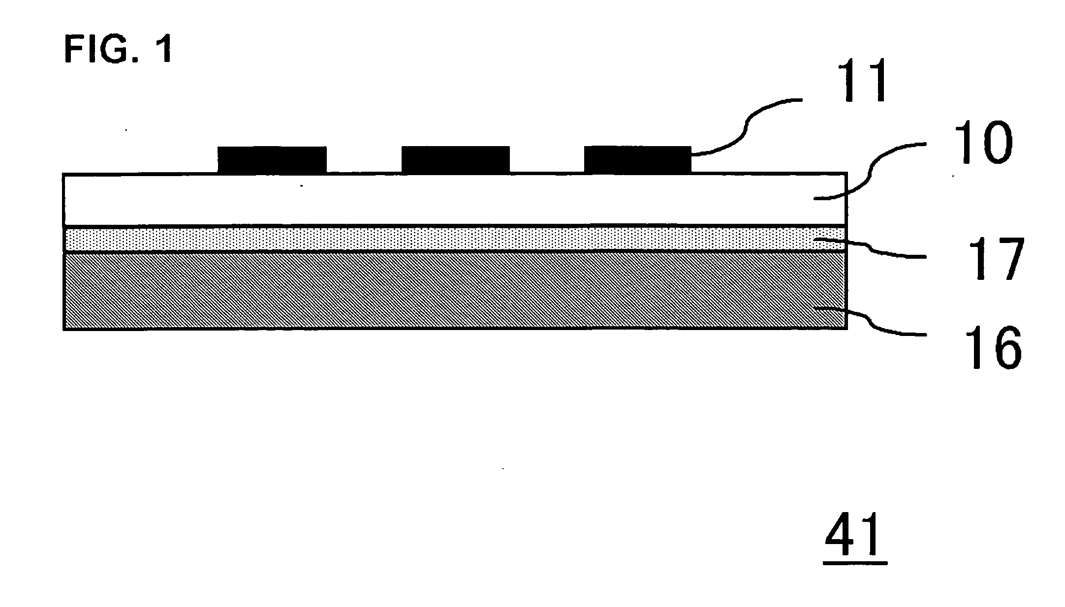
[0078]FIG. 1 is a diagram, showing a thin film device 41 according to the present embodiment. Thin film device 41 comprises a multiple-layered configuration that is formed of a film 16, an adhesive layer 17, a substrate 10 and semiconductor elements 11, which are layered in this sequence.

[0079] In the thin film device 41, a plurality of semiconductor elements 11 are provided on the surface of the substrate 10 to form an array-status. The semiconductor element 11 is appropriately selected according to an intended application of the thin film device 41, and may be, for example, a TFT such as a polysilicon TFT array, a thin film diode (TFD), metal wirings or the like.

[0080] The thickness of the semiconductor element 11 may be, for example, equal to or less than 200 μm, and preferably equal to or less than 100 μm. This can provide a device having a redu...

second embodiment

[0140] In method of first embodiment, a flush flow of an etchant solution may be supplied on the surface of the substrate 10 in the aforementioned process (iii), in stead of conducting an etching process while providing ultrasonic vibration. In addition, a stripping of the protective film 12 and an adhesion of the film 16 may be conducted by irradiating light. In this embodiment, a case of an electronic device having a TFT array and pixel electrodes will be illustrated.

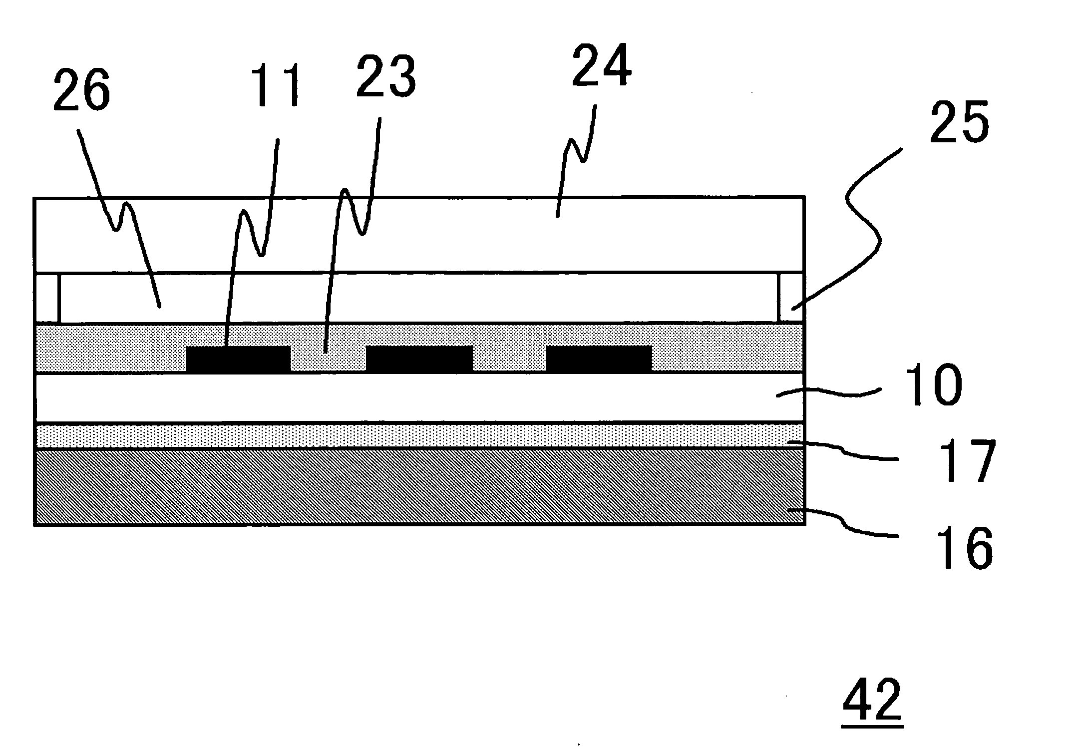
[0141]FIG. 4 is a cross-sectional view, schematically illustrating a configuration of a thin film device 42 according to the present embodiment. A basic configuration of the thin film device 42 is similar to the thin film device 41 shown in FIG. 1, and further comprises a multiple-layered configuration that is formed of a polyimide film 23, a liquid crystal 26, and a color filter substrate 24 which are layered in this order on the semiconductor element 11. The peripheral portions of the liquid crystal 26 are sealed b...

third embodiment

[0157] While the above-described embodiments employ the removal of a portion of the substrate 10 by the etching in the process step (iii), polishing processes such as a grinding process employing a grinding stone can be employed, instead of the etching process. Mechanical polishing may be employed, and chemical polishing may also be employed. Moreover, chemical mechanical polishing (CMP) may be employed.

[0158] While the second embodiment employs the photo-stripping cohesive agent 20 and the photo-setting adhesive layer 17, a thermally stripping adhesive may be employed for the adhesion of the protective film 12, and a thermosetting adhesive may also be used for the adhesive layer 17 that provides adhesion of the film 16. Description will be made in reference to a case of a flexible silicon-on-insulator (SOI) device.

[0159]FIG. 7 is a cross-sectional view, schematically illustrating a configuration of a thin film device 43 according to the present embodiment. A basic configuration o...


PUM

PropertyMeasurementUnit
thicknessaaaaaaaaaa
roughnessaaaaaaaaaa
curing shrinkageaaaaaaaaaa

Abstract

A method to provide an improved production yield of electronic devices. A thin film device 41 is manufactured by the following method. Semiconductor elements 11 are formed on the substrate 10. Then, a protective film is adhered onto the upper portions of the semiconductor elements 11 using an adhesive agent. Then, the substrate 10 is removed along the thickness direction from the surface thereof opposite to the surface having the semiconductor elements 11 provided thereon. Subsequently, a film 16 is adhered onto the surface of the removal-processed substrate 10. Subsequently, the protective film is removed. The obtained thin film device 41 is heat-treated.

Description

[0001] This application is based on Japanese patent application NO. 2004-217961, contents of which are incorporated hereinto by reference. BACKGROUND OF THE INVENTION [0002] 1. Field of the Invention [0003] The present invention relates to an electronic device and a method for manufacturing thereof. [0004] 2. Related Art [0005] In recent years, developments of flexible liquid crystal display devices employing resin substrates are proceeded, aiming at presenting thin film transistor liquid crystal display devices that have reduced weight and are resistant to breaking. As an implementation thereof, a method for forming a device has been developed, which involves transferring or copying a pattern of a thin film transistor (TFT) array, that is once formed on a glass substrate, on a resin substrate (Akihiko Asano and Tomoatsu Kinoshita, entitled “Low-Temperature Polycrystalline-Silicon TFT Color LCD Panel Made of Plastic Substrates”, Society for Information Display 2002, International Sy...

Claims


Application Information

Patent Timeline
Patent Type & Authority Applications(United States)
IPC IPC(8): H01L23/12H01L21/58
CPCG02F2001/13613H01L23/5387H01L27/1214H01L27/1266H05K3/386H01L2924/0002H01L2924/3511H05K2201/0145H01L2924/00G02F1/13613
Inventor EGUCHI, TOSHIMASATAKECHI, KAZUSHIGE
Owner SUMITOMO BAKELITE CO LTD
Why Eureka
Try Eureka