Switching power supply unit and semiconductor device for switching power supply

a technology of switching power supply and semiconductor device, which is applied in the direction of power conversion system, dc-dc conversion, instruments, etc., can solve the problems of insufficient power supply to the load under peak load, insufficient power supply to the secondary load, and insufficient power supply to the load, etc., to achieve no increase in component count, no increase in production cost, and no complex circuit configuration

Inactive Publication Date: 2006-01-26
COLLABO INNOVATIONS INC
View PDF5 Cites 37 Cited by
  • Summary
  • Abstract
  • Description
  • Claims
  • Application Information

AI Technical Summary

Benefits of technology

[0034] An object of the present invention is to provide a switching power supply unit and a semiconductor device for the switching power supply unit which have no increase in component count, entai...

Problems solved by technology

As described above, the maximum value of the primary drain current is fixed, so that a maximum power suppliable to the secondary load is limited.
However, there come up problems that when the maximum power limited under peak load is applied using ILIMIT, the power is too high as the overload protection level under normal load, and when ILIMIT is applied as the overload protection level under normal load, power cannot be sufficiently supplied ...

Method used


Image

  • Switching power supply unit and semiconductor device for switching power supply
  • Switching power supply unit and semiconductor device for switching power supply
  • Switching power supply unit and semiconductor device for switching power supply

Examples


first embodiment

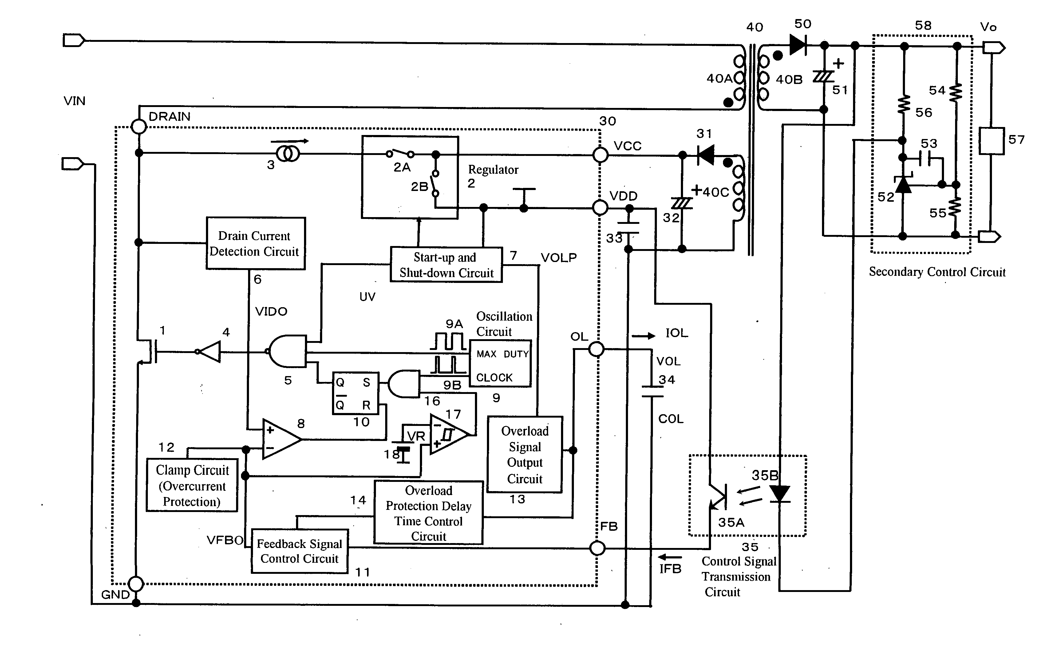
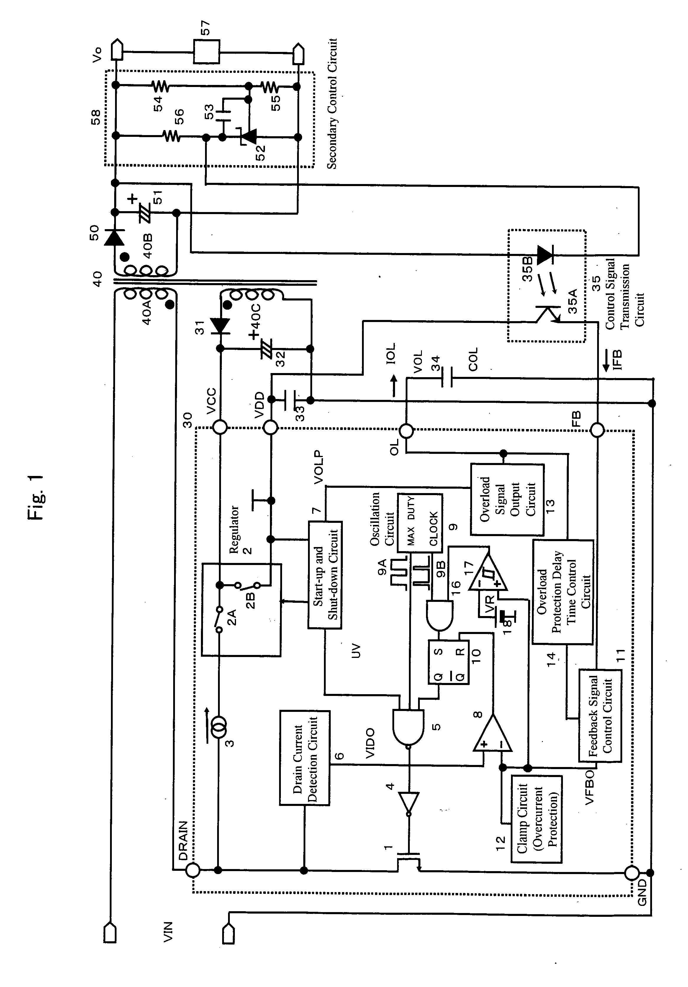
[0079]FIG. 1 is a circuit diagram of a switching power supply unit and a semiconductor device according to a first embodiment of the invention. FIG. 2 is a detailed circuit diagram for explaining the configuration of the semiconductor device 30 for controlling the switching power supply shown in FIG. 1.

[0080] In FIGS. 1 and 2, reference numeral 30 denotes the semiconductor device for controlling the switching power supply. The semiconductor device 30 includes a switching device 1 and its control circuit.

[0081] The semiconductor device 30 is provided with the input terminal (DRAIN) of the switching device 1, an auxiliary power supply voltage input terminal (VCC), an internal circuit power supply terminal (VDD), a feedback signal input terminal (FB), a capacitor connecting terminal (OL) for adjusting the delay time of overload protecting operation, the output terminal of the switching device 1, and the GND terminal (GND) of the control circuit as external input terminals.

[0082] Ref...

second embodiment

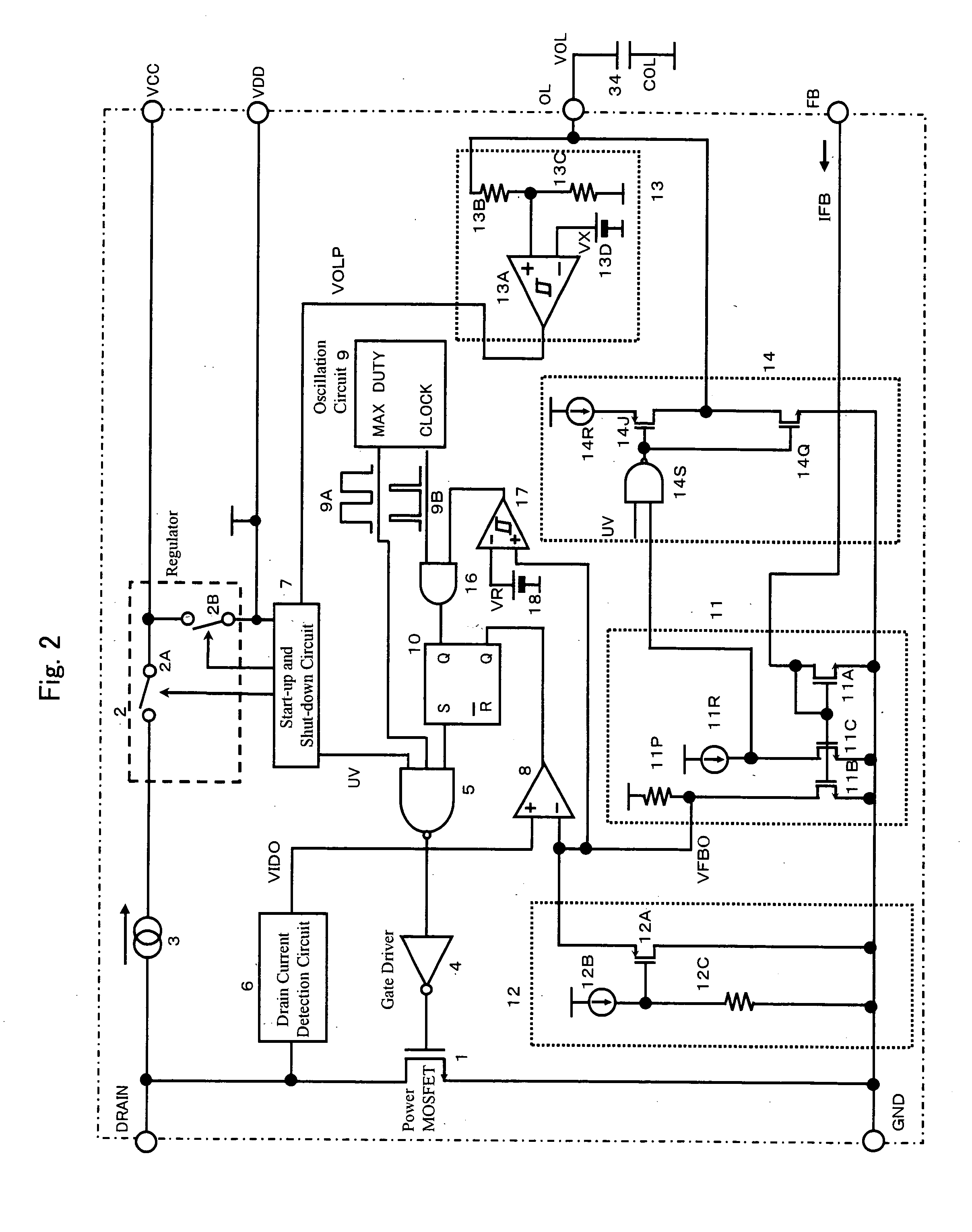
[0146]FIG. 6 is a circuit diagram of a semiconductor device for controlling a switching power supply included in a switching power supply unit according to a second embodiment of the invention. In FIG. 6, the internal circuit of the semiconductor device 30 shown in FIG. 1 is illustrated in detail, and since reference numerals correspond with those shown in FIG. 1, the explanation of the same component is omitted.

[0147] A difference between the configurations shown in FIGS. 6 and 2 is in components in the feedback signal control circuit. That is, as shown in FIG. 6, the feedback signal control circuit 11Y is provided with a comparator 11D and a reference voltage source 11E, the output signal VFBO of the feedback signal control circuit 11Y is input to the comparator 11D, and the output signal of the comparator 11D is input to the overload protection delay time control circuit 14.

[0148] Advantages obtained by adopting the configuration shown in FIG. 6 are as follows: when IFB2 at the...

third embodiment

[0149]FIG. 7 is a circuit diagram of a semiconductor device for controlling a switching power supply included in a switching power supply unit according to a third embodiment of the invention. In FIG. 7, the internal circuit of the semiconductor device 30 shown in FIG. 1 is illustrated in detail, and since reference numerals correspond with those shown in FIG. 1, the explanation of the same component is omitted.

[0150] A difference between the configurations shown in FIGS. 7 and 2 is in components in the overload signal output circuit. That is, as shown in FIG. 7, the overload signal output circuit 13Y is provided with a RS flip flop 13E which receives the output signal of the comparator 13A as a set signal. Furthermore, the RS flip flop 13E receives a reset signal VDDreset as an input. VDDreset refers to a reset signal from a component which does output when the input voltage used as power supply decreases, and then the terminal voltage VDD decreases below the specified voltage.

[0...


PUM


Abstract

Overload protecting operation is performed by controlling the current peak value of a switching device 1 through the use of a comparator 8, a NAND circuit 5, and so on according to variations in feedback current being input to a feedback signal control circuit 11, internally setting the overcurrent protection of switching device 1 through the use of a clamp circuit 12, charging a capacitor 34 when having fallen below a specified current smaller than current required for the overcurrent protection for a fixed time period, and detecting rise in voltage VOL at the capacitor 34 to a constant voltage to stop switching operation. By achieving the overload protection under normal load and the overcurrent protection against peak load in a single switching power supply unit, problems such as the complexity of the unit and an increase in the element count of the control circuit are solved.

Description

BACKGROUND OF THE INVENTION [0001] 1. Field of the Invention [0002] The present invention relates to a switching power supply unit having an overload protecting function and an overcurrent protecting function and to a semiconductor device used for the switching power supply unit. [0003] 2. Background Art [0004]FIG. 8 is a circuit diagram of an example of conventional switching power supply units. In FIG. 8, reference numeral 130 denotes a semiconductor device for controlling the switching power supply. The semiconductor device 130 includes a switching device 101 and its control circuit. [0005] The semiconductor device 130 is provided with the input terminal (DRAIN) of the switching device 101, an auxiliary power supply voltage input terminal (VCC), an internal circuit power supply terminal (VDD), a feedback signal input terminal (FB), the output terminal of the switching device 101, and the GND terminal (GND) of the control circuit as external input terminals. [0006] Reference numer...

Claims


Application Information

Patent Timeline
IPC IPC(8): H02M3/335
CPCH02M2001/0006H02M3/33523H02M1/0006
Inventor TAKAHASHI, SATORU
Owner COLLABO INNOVATIONS INC
Why Eureka
Try Eureka