

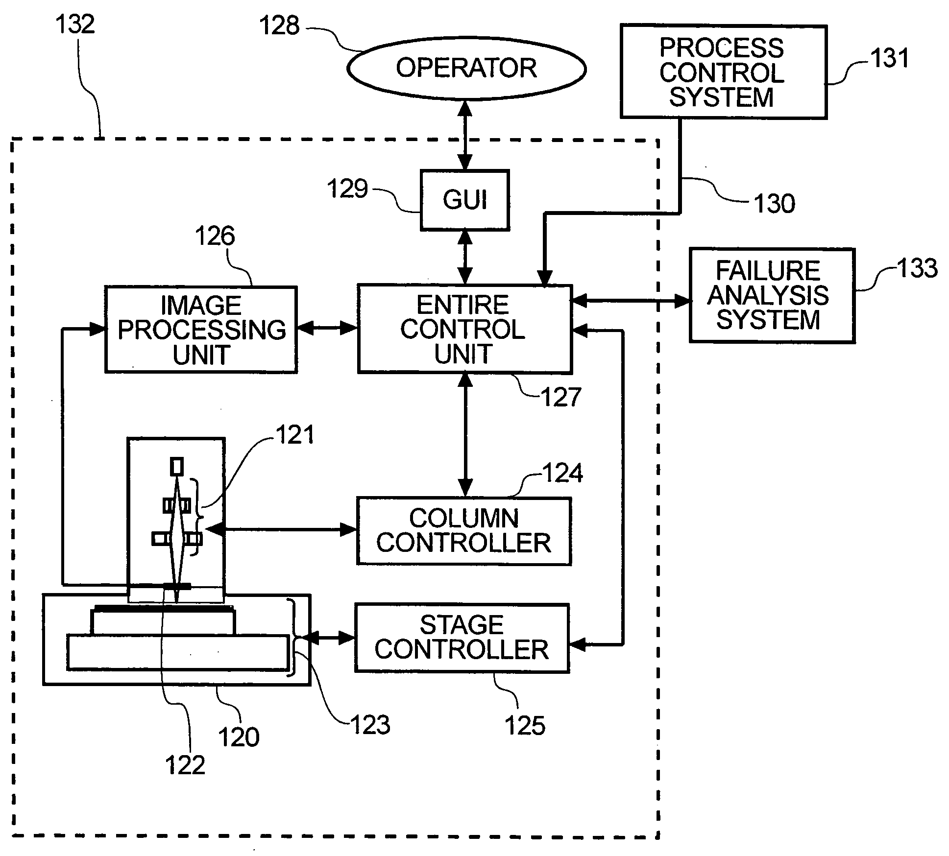
Method and apparatus for inspecting a semiconductor device
a semiconductor device and semiconductor technology, applied in semiconductor/solid-state device testing/measurement, instruments, television systems, etc., can solve the problems of large amount of defective units, and large amount of production, and achieve the effect of facilitating the determination of the cause of failures
- Summary
- Abstract
- Description
- Claims
- Application Information
AI Technical Summary
Benefits of technology
Problems solved by technology
Method used
Image

Examples
Embodiment Construction
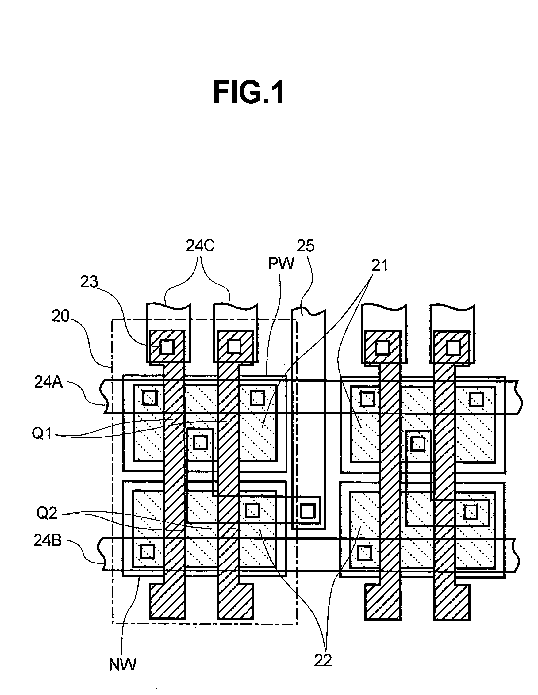
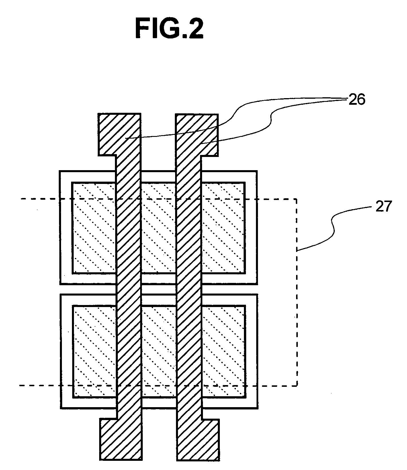
[0048]FIG. 1 shows an example of a logic unit of a semiconductor device, which is an object sample of the invention. This logic unit consists of a unit cell 20, which is enclosed with a phantom line in FIG. 1. The unit cell 20 consists of two n-channel MOS chips Q1 and two p-channel MOS chips Q2. The n-channel MOS chip Q1 is formed on an n-type region 21 in the surface of a p-WELL region PW formed on a substrate, and the p-channel MOS chip Q2 is formed on a p-type region 22 in the surface of an n-WELL region NM, respectively. Here, a plane view of a unit cell, before different types of traces 24A, 24B, 24C, and 25 are formed on it, is shown in FIG. 2. Reference numeral 26 denotes a polysilicon gate pattern. This unit cell is structured in such a way that 2-input NAND gates and 2-input NOR gate circuits can be formed efficiently by selecting traces to be subsequently added as necessary, and this structure is also extended to the structures connecting a large number of CMOS chips.
[00...
PUM
| Property | Measurement | Unit |
|---|---|---|
| threshold level | aaaaa | aaaaa |
| area | aaaaa | aaaaa |
| dimension | aaaaa | aaaaa |
Abstract
Description
Claims
Application Information