Optical or electronic module and method for its production

a technology production methods, applied in the field of optical or electronic modules, can solve the problems of damage to sensitive bonding wire connections, high thermal expansion coefficient of embedded materials, and inability to create optical paths within embedded materials, etc., and achieve the effect of improving the thermal properties of modules

Inactive Publication Date: 2006-02-09
AVAGO TECHNOLOGIED FIBER IP SINGAPORE PTE LTD
View PDF9 Cites 52 Cited by
  • Summary
  • Abstract
  • Description
  • Claims
  • Application Information

AI Technical Summary

Benefits of technology

[0018] According to one or more aspects of the present invention, a carrier is provided and the optical or electronic component is arranged on a first side of the carrier and at least one further component of the module is arranged on a second side of the carrier. In this case, the second region of the plastic package encapsulates the components arranged on the second side of the carrier. On the first side there is exclusively the transparent polymer compound. This division allows simple application of the polymer compounds and production of the module. Alternatively, however, the second region of the plastic package also partly extends onto the first side of the carrier, but does not cover the first region with the transparent polymer compound.
[0019] As a result, the thermal properties of the module are further improved. According to one or more aspects of the present invention, the optical or electronic component is preferably arranged on the carrier by means of a printed circuit board with via holes. The printed circuit board consists, for example, of customary printed circuit board material or a patterned film of plastic (e.g., of Kapton®).

Problems solved by technology

However, the use of embedding materials that are transparent for the respective range of wavelengths has disadvantages in that transparent embedding materials generally have a high coefficient of thermal expansion and, accordingly, when there are great temperature fluctuations, stresses can occur within the embedding or pachaging materials which can damage sensitive bonding wire connections.
A general disadvantage of the use of such polymers, however, is that an optical path cannot be created within the embedding material.

Method used


Image

  • Optical or electronic module and method for its production
  • Optical or electronic module and method for its production
  • Optical or electronic module and method for its production

Examples


Embodiment Construction

[0039] One or more aspects of the present invention will now be described with reference to the drawing figures, wherein like reference numerals are used to refer to like elements throughout. It should be understood that the drawing figures and following descriptions are merely illustrative and that they should not be taken in a limiting sense. In the following description, for purposes of explanation, numerous specific details are set forth in order to provide a thorough understanding of the present invention. It will be evident to one skilled in the art, however, that the present invention may be practiced without these specific details. Thus, it will be appreciated that variations of the illustrated systems and methods apart from those illustrated and described herein may exist and that such variations are deemed as falling within the scope of the present invention and the appended claims.

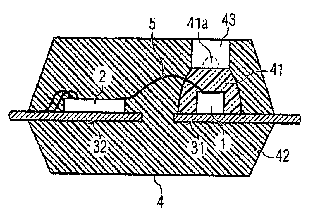
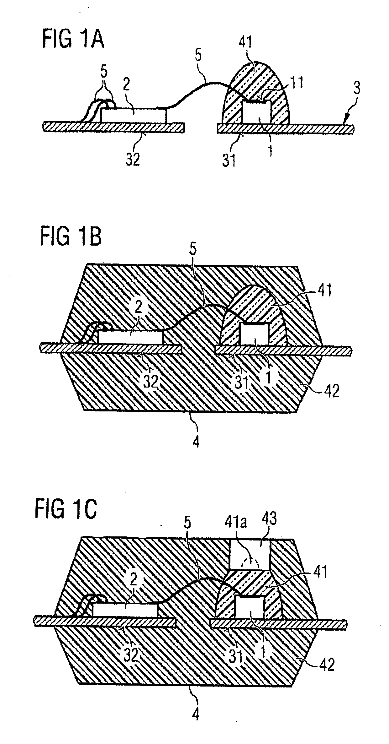
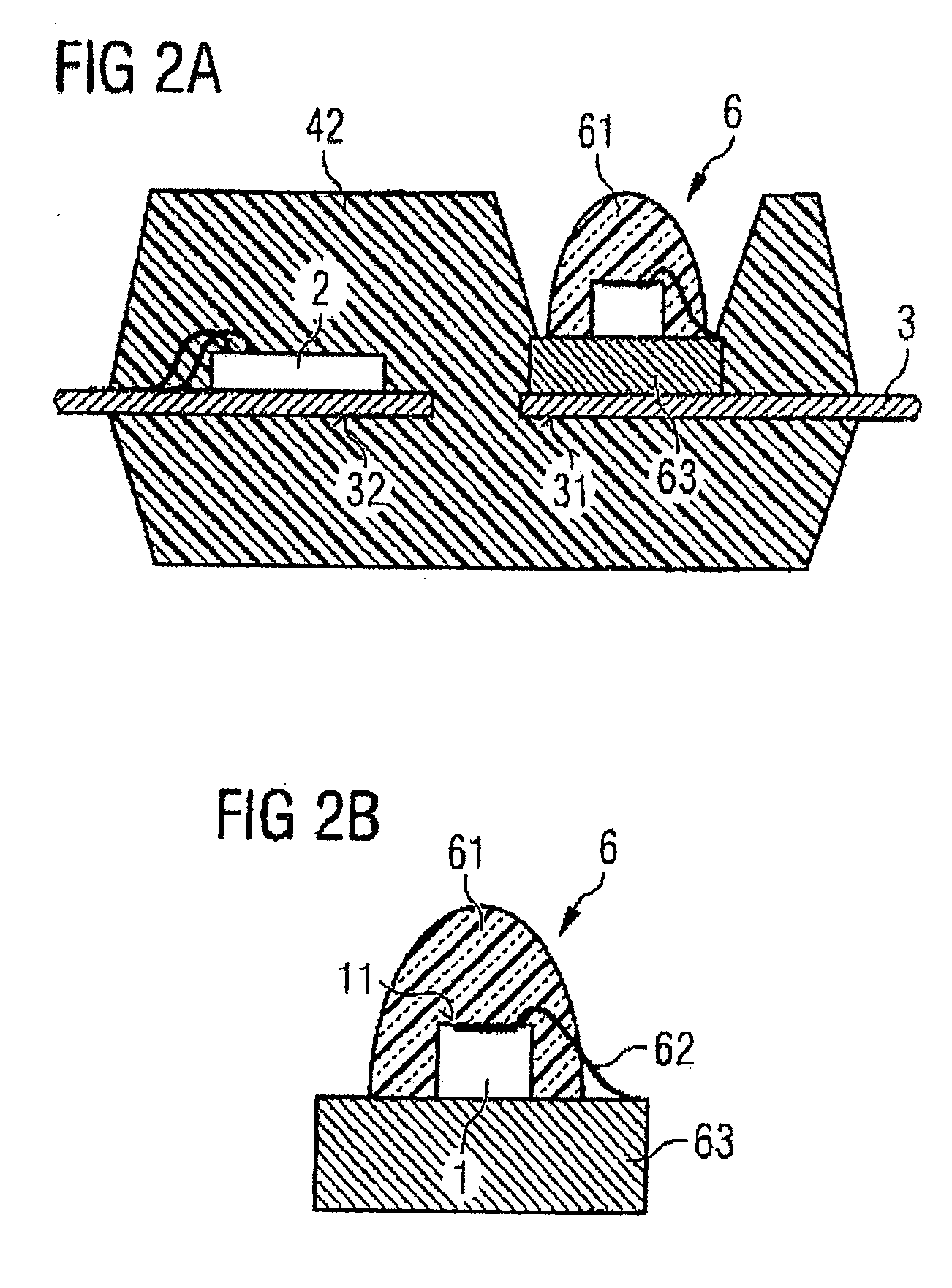
[0040]FIG. 1c illustrates a first exemplary embodiment of an optical module according to on...


PUM


Abstract

One or more aspects of the invention relate to an optical or electronic module with at least one optical or electronic component and a plastic package within which the component is embedded. The component has an operative region that facilitates operative connection with surroundings. The plastic package has a first region, which comprises a transparent polymer compound, and a second region, which comprises a non-transparent polymer compound. The first region extends such that it borders the operative region of the component.

Description

REFERENCE TO RELATED APPLICATIONS [0001] This application claims the benefit of the priority date of European application 04090300.7, filed on Jul. 28, 2004, the contents of which are herein incorporated by reference in their entirety. FIELD OF THE INVENTION [0002] The present invention relates generally optics, and more particularly to an optical or electronic module and one or more techniques for making the same. BACKGROUND OF THE INVENTION [0003] It is known to embed optoelectronic modules with a transparent embedding material. For example, DE 199 09 242 A1 discloses an optoelectronic module where a leadframe with an optoelectronic transducer is positioned in a module package and embedded with a transparent, moldable polymer material. Light is coupled in or out by means of an optical fiber, which is coupled to a connecting piece of the module package. On the leadframe there is also a driver device or receiving device for the optoelectronic transducer. [0004] However, the use of e...

Claims


Application Information

Patent Timeline
Patent Type & Authority Applications(United States)
IPC IPC(8): B65D65/00H01L33/54H01S5/0232
CPCG02B6/4201G02B6/4204H01L2924/12041H01L2924/01068H01L24/49H01L24/48H01S5/02244H01S5/02216H01L2924/19041H01L2924/1815H01L2924/14H01L2224/8592H01L23/3135H01L23/49575H01L25/167H01L33/54H01L2224/48091H01L2224/48137H01L2224/48235H01L2224/48247H01L2224/48472H01L2224/49109H01L2924/00014H01L2924/00H01L2924/12043H01L2924/181H01L2224/48257G02B6/4253G02B6/426G02B6/4245G02B6/4257G02B6/4274H01S5/0231H01S5/0232H01L2924/00012H01L2224/45099H01L2224/45015H01L2924/207
Inventor AUBURGER, ALBERTHURT, HANSLICHTENEGGER, THOMASPAULUS, STEFANSCHUNK, NIKOLAUSWEBERPALS, FRANKWITTL, JOSEF
Owner AVAGO TECHNOLOGIED FIBER IP SINGAPORE PTE LTD
Why Eureka
Try Eureka