Semiconductor device including a high-breakdown voltage MOS transistor

a technology of mos transistor and semiconductor device, which is applied in the direction of semiconductor devices, electrical apparatus, transistors, etc., can solve the problems of undesirable pattern layout area of the semiconductor device as a whole, undesirable conventional semiconductor devices described above, and achieve the effect of suppressing the increase in the pattern layout area of the semiconductor devi

Inactive Publication Date: 2006-02-09
RENESAS ELECTRONICS CORP
View PDF33 Cites 17 Cited by
  • Summary
  • Abstract
  • Description
  • Claims
  • Application Information

AI Technical Summary

Benefits of technology

[0022] By this structure, first, an MOS transistor including the second impurity region, the third impurity region, the fourth impurity region and the electrode portion is formed. The second impurity region of the MOS transistor also serves as a resistance element, and therefore, it follows that a resistance element is connected in seri

Problems solved by technology

The conventional semiconductor device described above, however, has the following problems.
As the pattern is arranged repeatedly, the area occupied by the pattern on the semiconductor substrate becomes

Method used


Image

  • Semiconductor device including a high-breakdown voltage MOS transistor
  • Semiconductor device including a high-breakdown voltage MOS transistor
  • Semiconductor device including a high-breakdown voltage MOS transistor

Examples


first embodiment

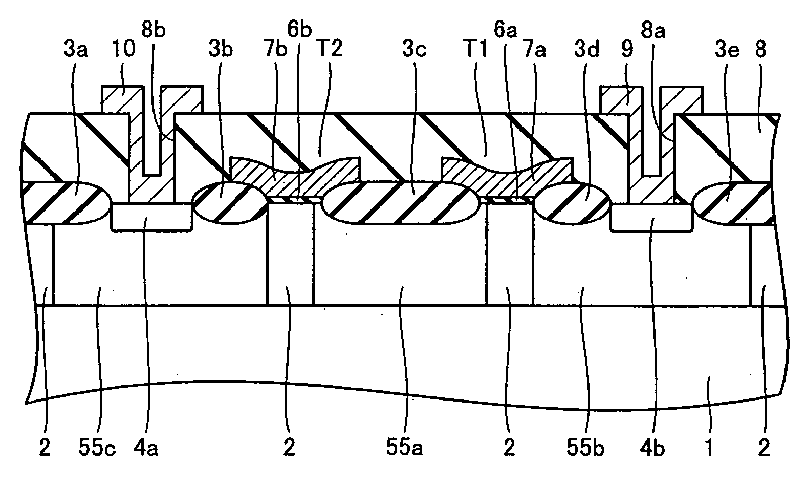
[0045] A semiconductor device including a high-breakdown voltage MOS transistor in accordance with a first embodiment will be described. As can be seen from FIGS. 1 and 2, on a semiconductor substrate 1, a well 2 as a first impurity region is formed. At prescribed regions of the surface of well 2, element isolating insulation films 3a to 3e are formed, respectively.

[0046] On the surface of well 2 sandwiched by element isolating insulation films 3a and 3b, a drain region 4a as a fourth impurity region is formed. In that region of well 2 which is immediately below element isolating insulation films 3a, 3b, a drain field limiting layer 5c as the fourth impurity region is formed to limit electric field of the drain.

[0047] On the surface of well 2 sandwiched by element isolating insulation films 3d and 3e, a source region 4 as a third impurity region is formed. In that region of well 2 which is immediately below element isolating insulation films 3d, 3e, a source field limiting layer 5...

second embodiment

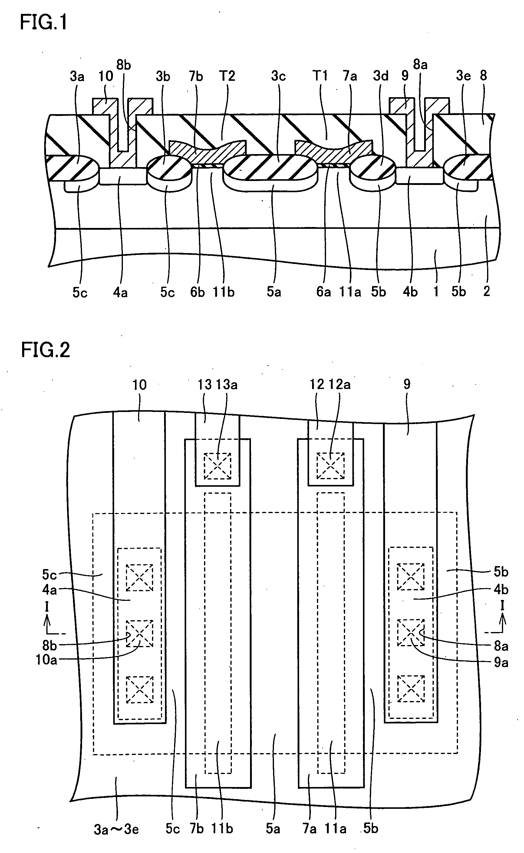
[0059] In the foregoing, a semiconductor device has been described in which drain field limiting layer 5c, source / drain region 5a and source field limiting layer 5b are formed at those portions of well region 2 which are positioned immediately below element isolating insulation films 3a to 3e.

[0060] Here, an example will be described in which the drain field limiting layer, the source / drain region and the source field limiting layer are formed as wells.

[0061] As shown in FIGS. 5 and 6, at regions immediately below element isolating insulation films 3a and 3b and drain region 4a, a well 55c reaching the surface of semiconductor substrate 1 is formed.

[0062] At a region immediately below element isolating insulation film 3c, a well 55a reaching the surface of semiconductor substrate 1 is formed. Further, at a region immediately below element isolating insulation films 3d, 3e and source region 4b, a well 55b reaching the surface of semiconductor substrate 1 is formed. Semiconductor s...

third embodiment

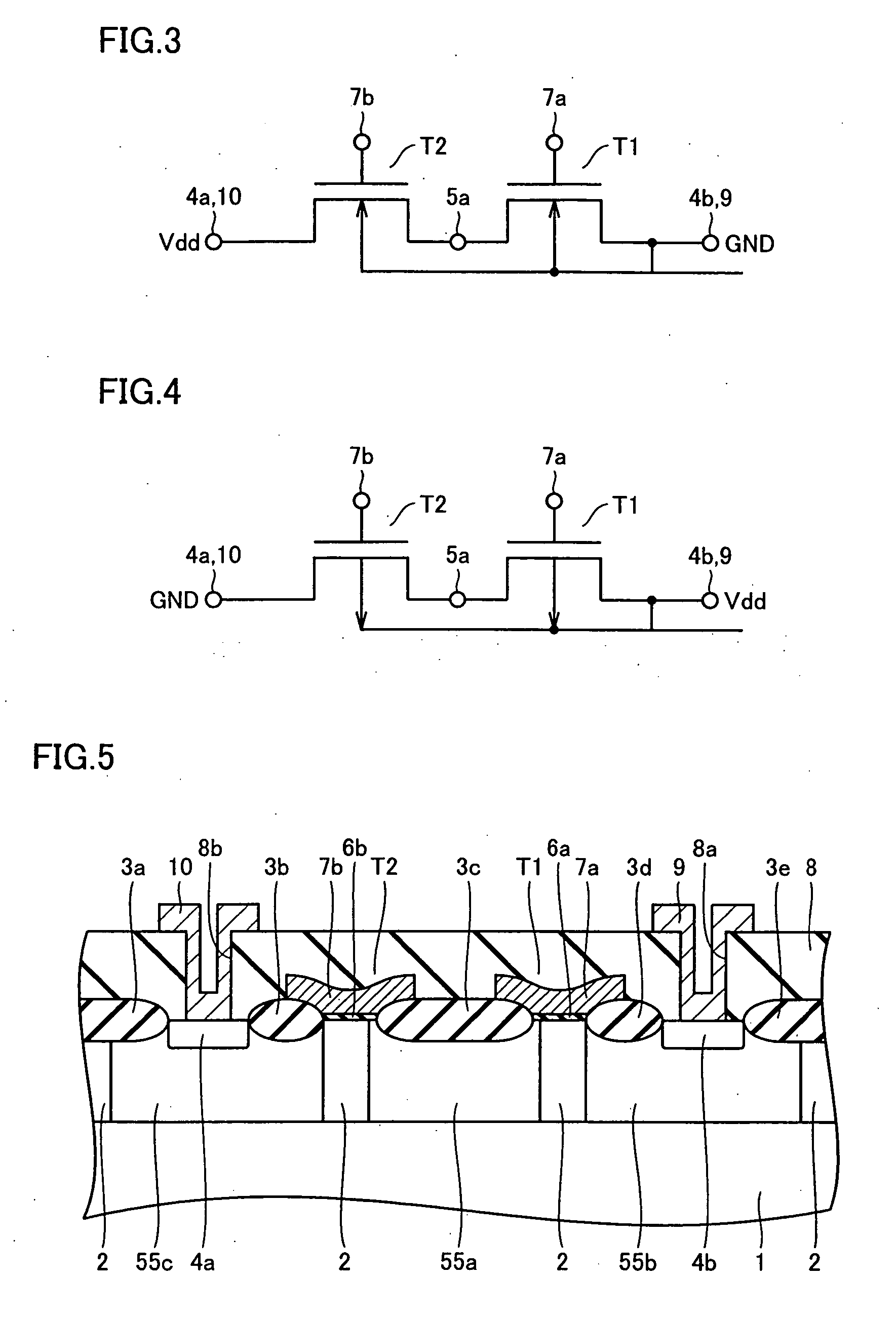
[0068] Here, a semiconductor device will be described as an example, in which two MOS transistors having mutually different gate widths (channel widths) are connected in series.

[0069] Referring to FIG. 8, channel W1 of MOS transistor T1 is made shorter than channel W2 of MOS transistor T2. Source / drain region 5a has its width along the direction of extension of gate electrodes 7a and 7b changed smoothly at a portion from the side of channel region 11b to the side of channel region 11a, as denoted by the portion A surrounded by dotted lines.

[0070] Except for these points, the semiconductor device is the same as that of FIG. 1, and therefore, corresponding portions are denoted by the same reference characters and description thereof will not be repeated.

[0071] By the above described semiconductor device, the following effect can be obtained in addition to the effects described with reference to the first embodiment.

[0072] First, MOS transistors T1 and T2 have channel widths W1 and...


PUM


Abstract

On a semiconductor substrate, a well is formed. In the well, one MOS transistor including a gate electrode, a source region, a source field limiting layer and a source/drain region, and another MOS transistor including a gate electrode, a drain electrode, a drain field limiting layer and a source/drain region are formed. The one and another MOS transistors are connected in series through the source/drain region common to the two transistors. Accordingly, a semiconductor device can be provided in which increase in pattern layout area is suppressed when elements including a high-breakdown voltage MOS transistor are to be connected in series.

Description

BACKGROUND OF THE INVENTION [0001] 1. Field of the Invention [0002] The present invention relates to a semiconductor device and, more specifically, to a semiconductor device including a high-breakdown voltage MOS transistor. [0003] 2. Description of the Background Art [0004] Semiconductor devices having a high-breakdown voltage MOS (Metal Oxide Semiconductor) transistor applied to a logic circuit or an analog circuit, have been known. As an example of such a semiconductor device, a semiconductor device disclosed in Japanese Patent Laying-Open No. 2001-94103 will be described. [0005] In the semiconductor device described in this laid-open application, in one of prescribed regions on a semiconductor substrate, an n-channel type high-breakdown voltage MOS transistor is formed. [0006] First, in a P-type semiconductor device, a P-type well is formed. The P-type well is a well diffusion layer for the high-breakdown voltage MOS transistor. On the P-type well, a gate electrode is formed wit...

Claims


Application Information

Patent Timeline
IPC IPC(8): H01L29/94H01L29/76H01L21/8234H01L21/82H01L27/07H01L27/088H01L29/78
CPCH01L27/0705Y10S257/917H01L27/088H01L29/7831H01L29/42368H01L29/78
Inventor TAYA, MASATOSHI
Owner RENESAS ELECTRONICS CORP
Why Eureka
Try Eureka