

Metallization layers for crack prevention and reduced capacitance
a technology of metalization layers and crack prevention, applied in semiconductor devices, semiconductor/solid-state device details, electrical devices, etc., can solve the problems of reducing the size of the rc time constant, the effect of signal delay becoming critical, and the difficulty of providing interconnection technology, etc., to achieve the effect of improving the resistance to cracking
- Summary
- Abstract
- Description
- Claims
- Application Information
AI Technical Summary
Benefits of technology
Problems solved by technology
Method used
Image

Examples
Embodiment Construction
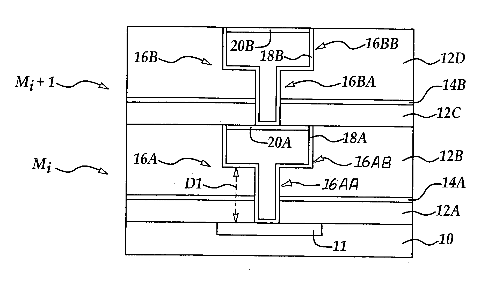
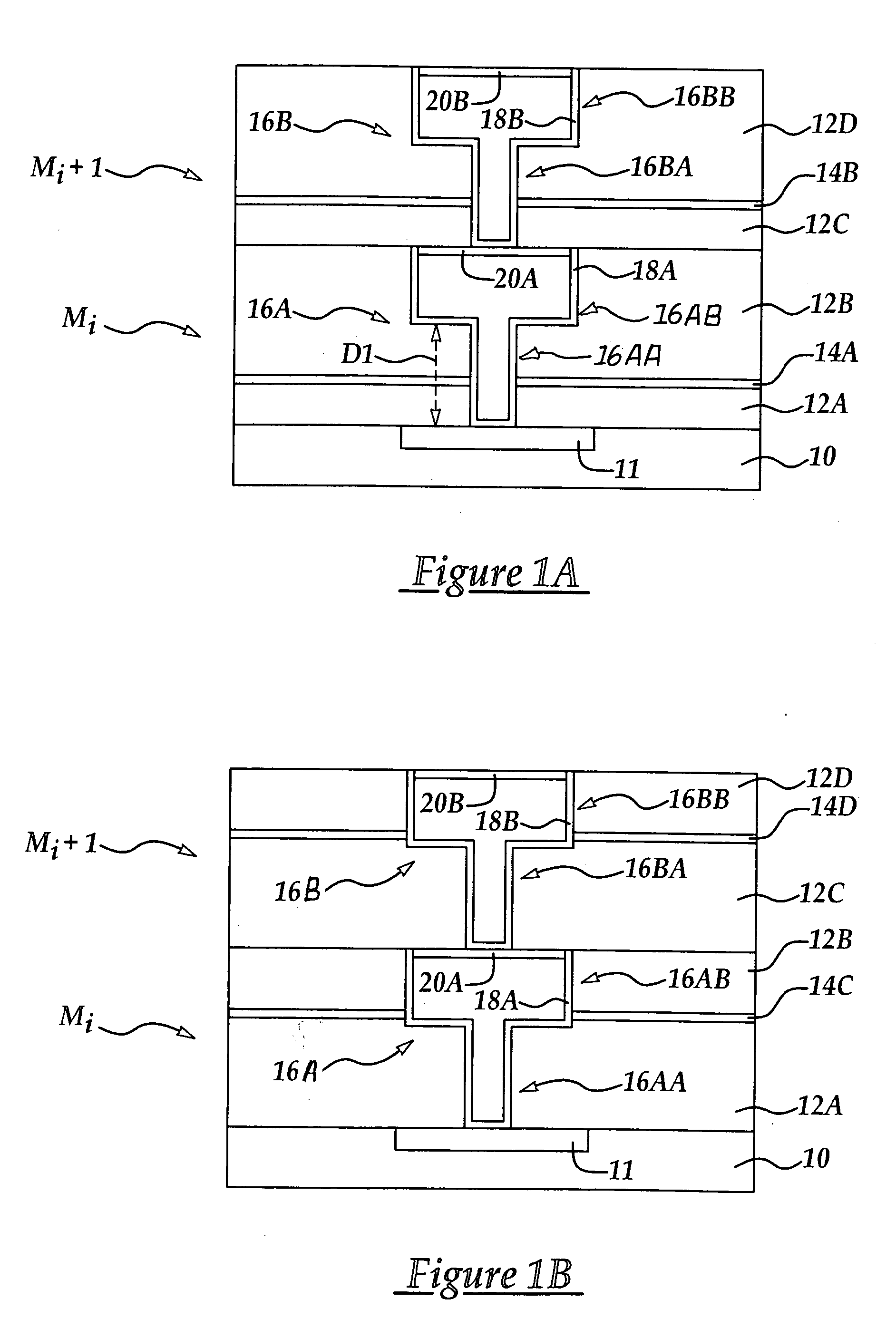
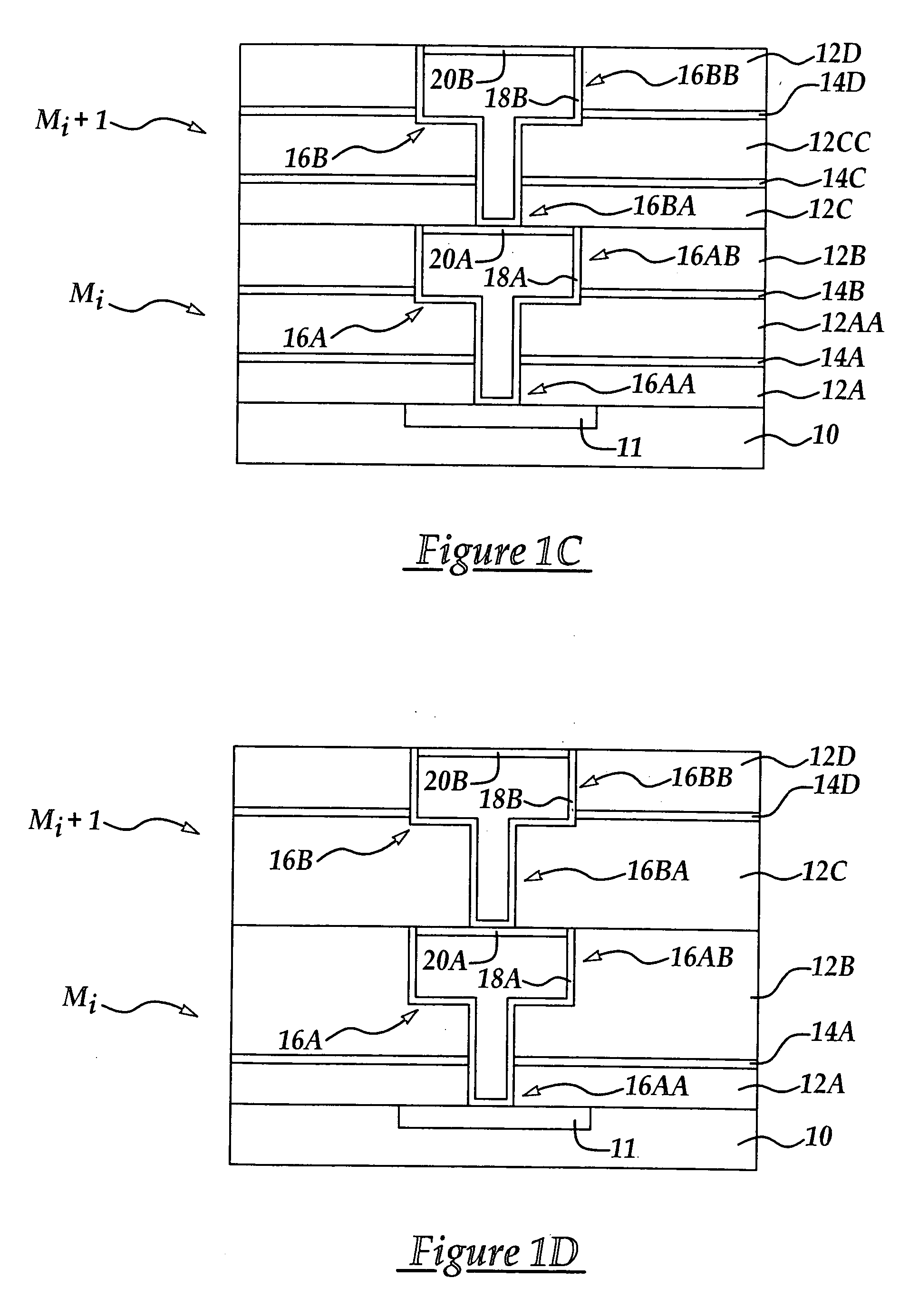
[0015] Although the method of the present invention is explained by exemplary reference the formation of a dual damascene structure according to a via-first method of formation in a multi-level semiconductor device it will be appreciated that the method of the present invention is equally applicable to other methods of dual or single damascene structure formation including for example stacked vias and damascene structures such as bonding pads. While the method of the present invention is particularly advantageously implemented with respect to copper filled dual damascene structures, it will be appreciated that the method may be adapted for use with other metal fillings, for example including tungsten, aluminum, and copper and alloys thereof. Further, the term ‘copper’ will be understood to include copper and alloys thereof.
[0016] For example, referring to FIG. 1A is shown a schematic representation of a cross sectional portion of a multi-level semiconductor device formed according ...
PUM
| Property | Measurement | Unit |
|---|---|---|
| thickness | aaaaa | aaaaa |
| dielectric constant | aaaaa | aaaaa |
| dielectric constant | aaaaa | aaaaa |
Abstract
Description
Claims
Application Information