
Semiconductor package, printed board mounted with the same, and electronic apparatus having the printed board

a technology of printed board and semiconductor, applied in the direction of semiconductor devices, semiconductor/solid-state device details, electrical devices, etc., can solve the problems of heat radiation effect deterioration

Inactive Publication Date: 2006-02-16
FUJITSU LTD
View PDF12 Cites 5 Cited by
  • Summary
  • Abstract
  • Description
  • Claims
  • Application Information

AI Technical Summary

Benefits of technology

[0008] Accordingly, it is an exemplary object to provide a semiconductor package, a printed board having the semiconductor package, and an electronic apparatus, which thermally protects the exoergic element and jointing layer due to the thermal stress associated with the junction with the heat spreader, while maintaining the heat radiation effect for the exoergic element.
[0009] A semiconductor package according to one aspect of the present invention that can be mounted on a printed board includes a package board that is mounted with an exoergic circuit element, a heat spreader that transmits heat from the exoergic circuit element, and a jointing layer that joints the exoergic circuit element to the heat spreader and is made of a solid jointing material that has substantially no elasticity, wherein the heat spreader includes a first surface jointed to the exoergic circuit element, and a second surface as a rear surface of the first surface, and wherein the heat spreader has a slit that extends in a substantially radial direction from an inner side to an outer side with respect to a first area that is jointed to the exoergic circuit element on the first surface or a second area that is an orthogonal projection of the first area onto the second surface, when the heat spreader is transparently viewed from the first or second surface. The slits enables the heat spreader of the semiconductor package to easily deform, and reduces the residue stress that affects the exoergic circuit element after the jointing layer made of a epoxy resin or another metal jointing material, such as solder, is hardened. On the other hand, the metal jointing material, such as solder, which has a large coefficient of thermal conductivity strongly adheres the exoergic circuit element made of silicon, etc. to the heat spreader made of copper having a large coefficient of thermal conductivity, and improve the heat radiation efficiency.
[0010] Preferably, plural slits are arranged substantially symmetrical with respect to a center of the exoergic circuit element, like a substantially cross or asterisk shape. The symmetry can prevent the stress from partially concentrating on the exoergic circuit element. The slit may perforate through the heat spreader. Since the slit assists the heat spreader in deforming, its shape, size and the number are not limited as long as the heat radiation efficiency can be maintained. In other words, as the slit area is larger, the heat spreader becomes easily deformable. However, it is preferable that the slit is spaced from a center of the exoergic circuit element by a predetermined distance. This is because that the center of the exoergic circuit element is generally a heat source, and the heat radiation effect can deteriorate greatly if the slit is formed in the center.

Problems solved by technology

This is because that the center of the exoergic circuit element is generally a heat source, and the heat radiation effect can deteriorate greatly if the slit is formed in the center.
Preferably, the slit substantially follows beat flux of the heat, formed on the heat spreader, because the heat radiation effect can deteriorate greatly if the slit crosses the heat flux for radiating the exoergic circuit element.

Method used


Image

  • Semiconductor package, printed board mounted with the same, and electronic apparatus having the printed board
  • Semiconductor package, printed board mounted with the same, and electronic apparatus having the printed board
  • Semiconductor package, printed board mounted with the same, and electronic apparatus having the printed board

Examples


Embodiment Construction

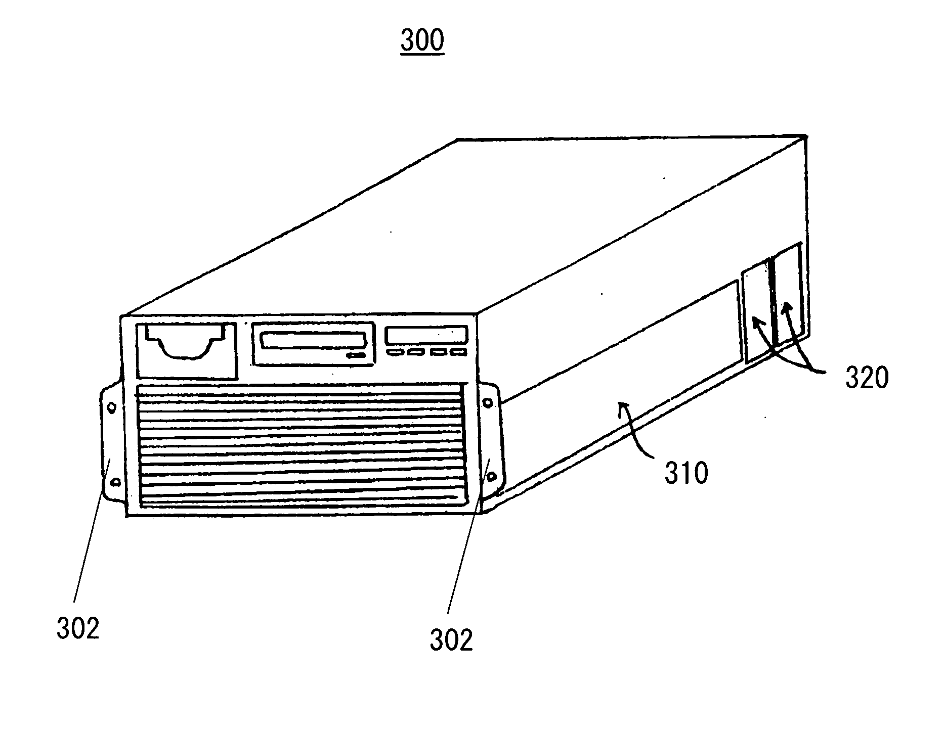
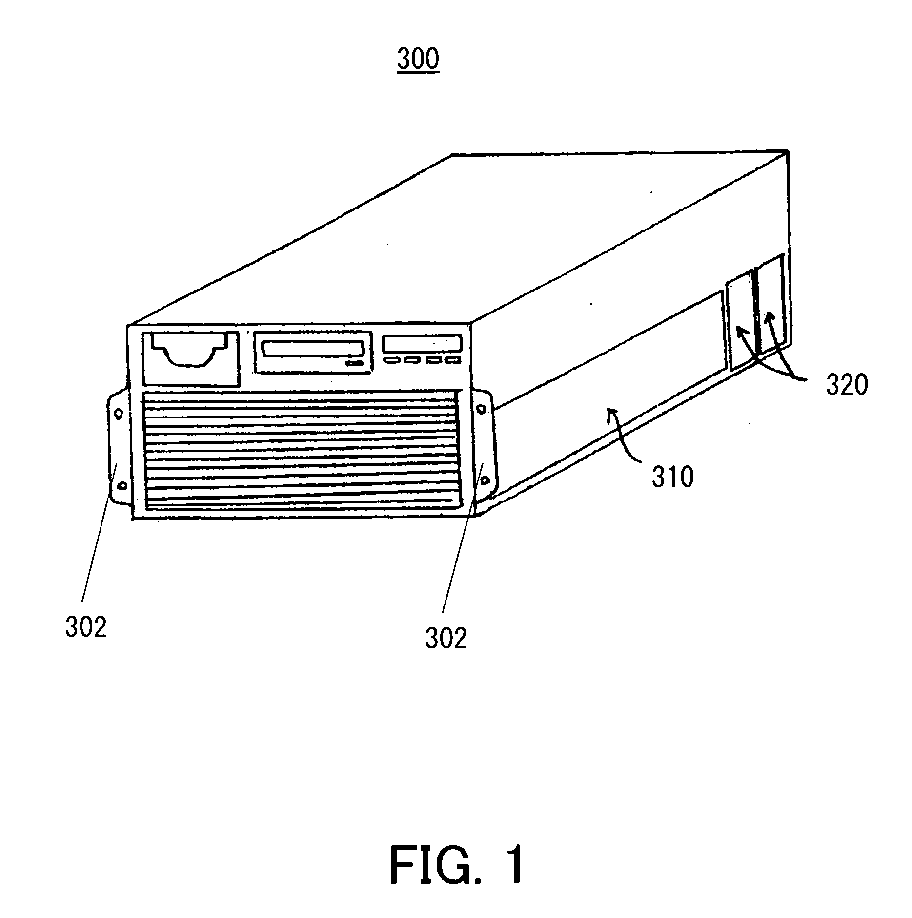
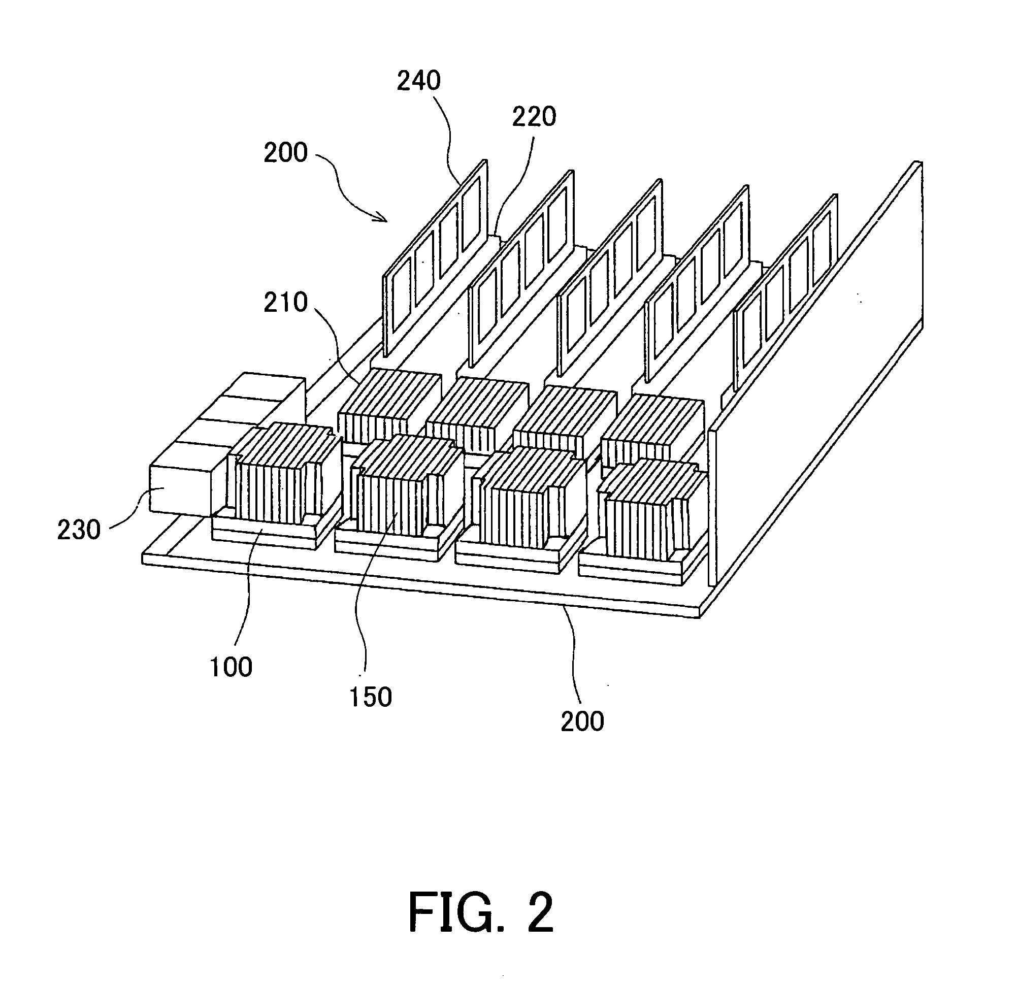
[0022] Referring now to accompanying drawings, a description will be given of a package module 100 as a semiconductor package according to one embodiment of the present invention, a printed circuit board 200 mounted with the package module 100, and an electronic apparatus 300 that includes the printed circuit board 200. Here, FIG. 1 is a schematic perspective view of the electronic apparatus 300. FIG. 2 is a perspective overview of a system board as the printed circuit board 200 included in the electronic apparatus 300.

[0023] As shown in FIG. 1, the electronic apparatus 300 of the instant embodiment is exemplarily implemented as a rack mount type UNIX server. The electronic apparatus 300 is screwed onto a rack (not shown) by a pair of attachment parts 302, and includes the printed circuit board 200 shown in FIG. 2 in a housing 310.

[0024] The housing 310 is provided with a fan module 320, which rotates a built-in cooling fan to generate airflow and compulsorily cools a heat sink 15...


PUM


Abstract

A holding fixture that holds a component and mounts the component on an electronic circuit board includes a holding member that holds the component at a side of a first surface of the electronic circuit board, a first fixing member that includes a first base that is engageable with the holding member, and an elastic member that is pivotally attached to the base, sandwiches the electronic circuit board at a side of a second surface of the electronic circuit board, and elastically supports the holding member at the side of the first surface, the second surface opposing to the first surface, and a second fixing member that includes a second base that is engageable with the holding member, and a projection member that projects from the second surface of the electronic circuit board and is engageable with the elastic member.

Description

[0001] This application claims the right of foreign priority under 35 U.S.C. §119 based on Japanese Patent Application No. 2004-232921, filed Aug. 10, 2004, which is hereby incorporated by reference herein in its entirety as if fully set forth herein. BACKGROUND OF THE INVENTION [0002] The present invention relates generally to a heat radiating mechanism, and more particularly to a heat radiating mechanism that transmits the heat generated from an exoergic circuit element (referred to as “exoergic element” hereinafter) mounted on an electronic apparatus. The present invention is suitable, for example, for a heat spreader that radiates a CPU mounted on a printed board (also referred to as a “system board” or “motherboard”) in a personal computer (referred to as “PC” hereinafter). Here, the “heat spreader” is a metal plate that efficiently transmits the heat from the exoergic element to the outside. [0003] A Ball Grid Array (“BGA”) package, one type of package board soldered to the pr...

Claims


Application Information

Patent Timeline
Patent Type & Authority Applications(United States)
IPC IPC(8): H01L23/34
CPCH01L23/36H01L23/367H01L2924/0002H01L2924/00
Inventor ANZAI, HISAO
Owner FUJITSU LTD
Learn More