

Pixel for CMOS image sensor having a select shape for low pixel crosstalk
- Summary
- Abstract
- Description
- Claims
- Application Information
AI Technical Summary
Benefits of technology
Problems solved by technology
Method used
Image

Examples
Embodiment Construction
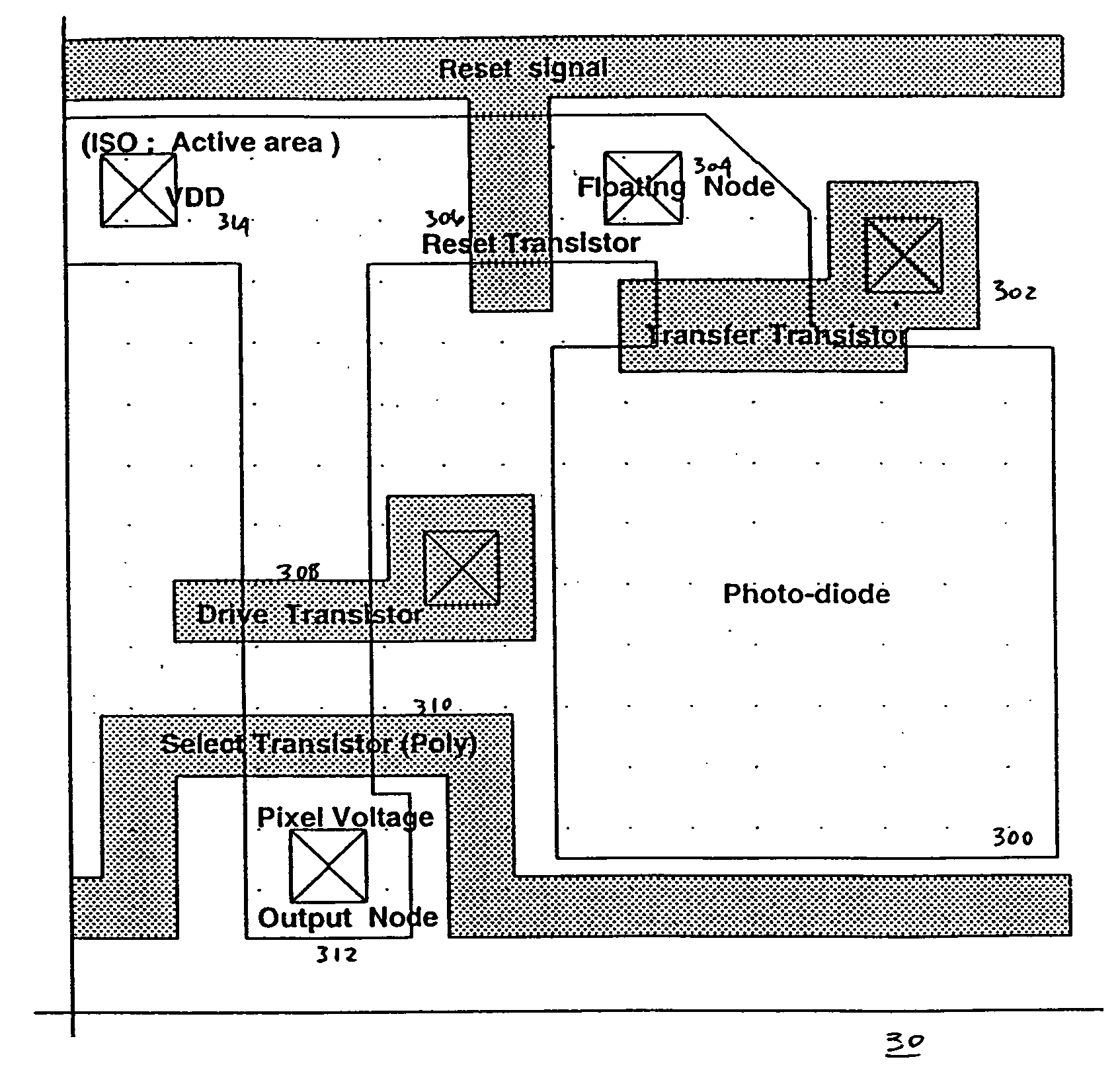
[0024] Referring to FIG. 3, there is shown a layout view of a specific embodiment of a unit pixel 30 for a CMOS image sensor according to the present invention. Unit pixel 30 is comprised of a square-shaped image sensing area 300, transfer transistor 302, floating node 304, reset transistor 306, drive transistor 308, select transistor 310 and output 312. Unit pixel 30 is powered by power supply VDD 314.
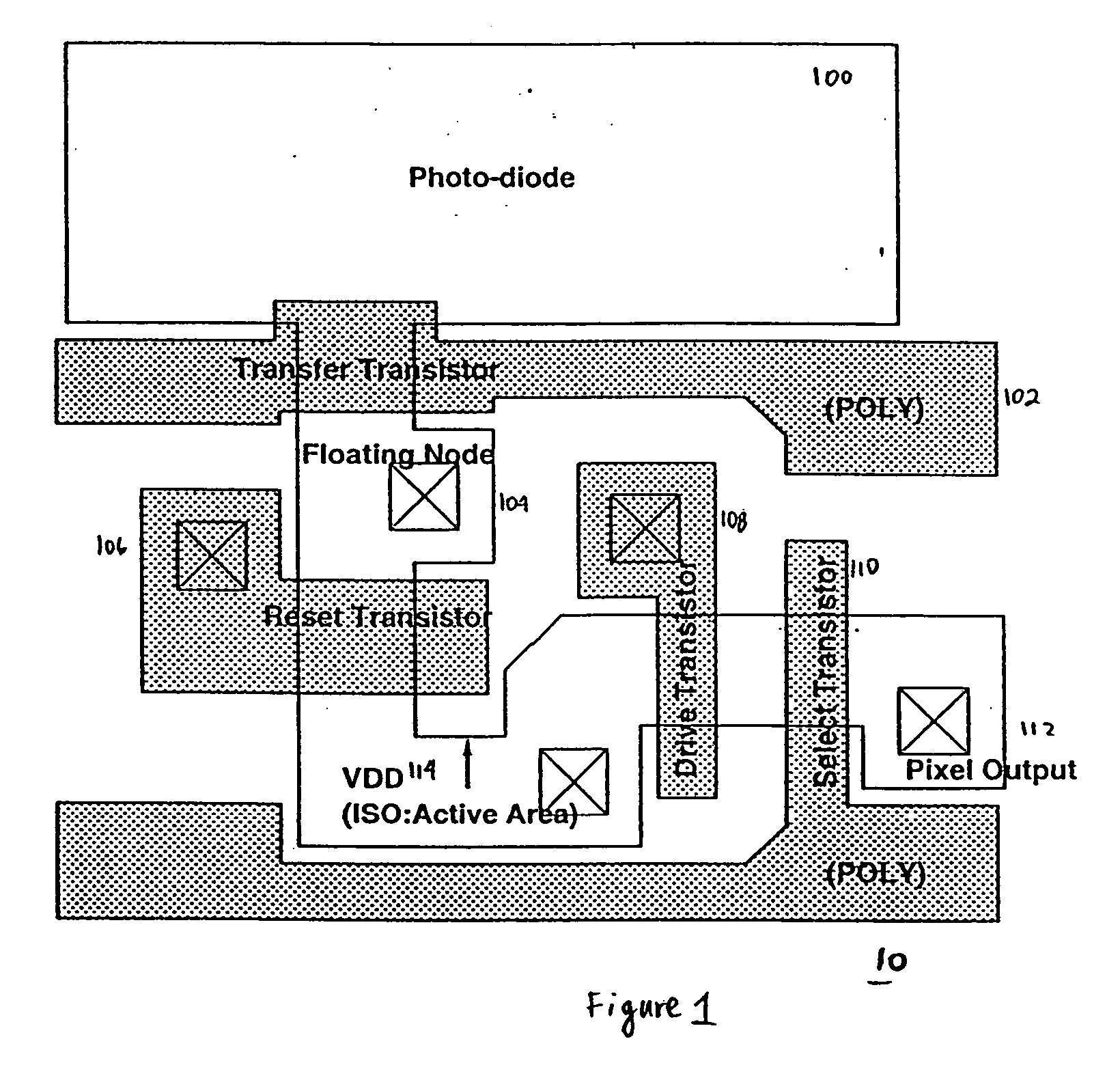
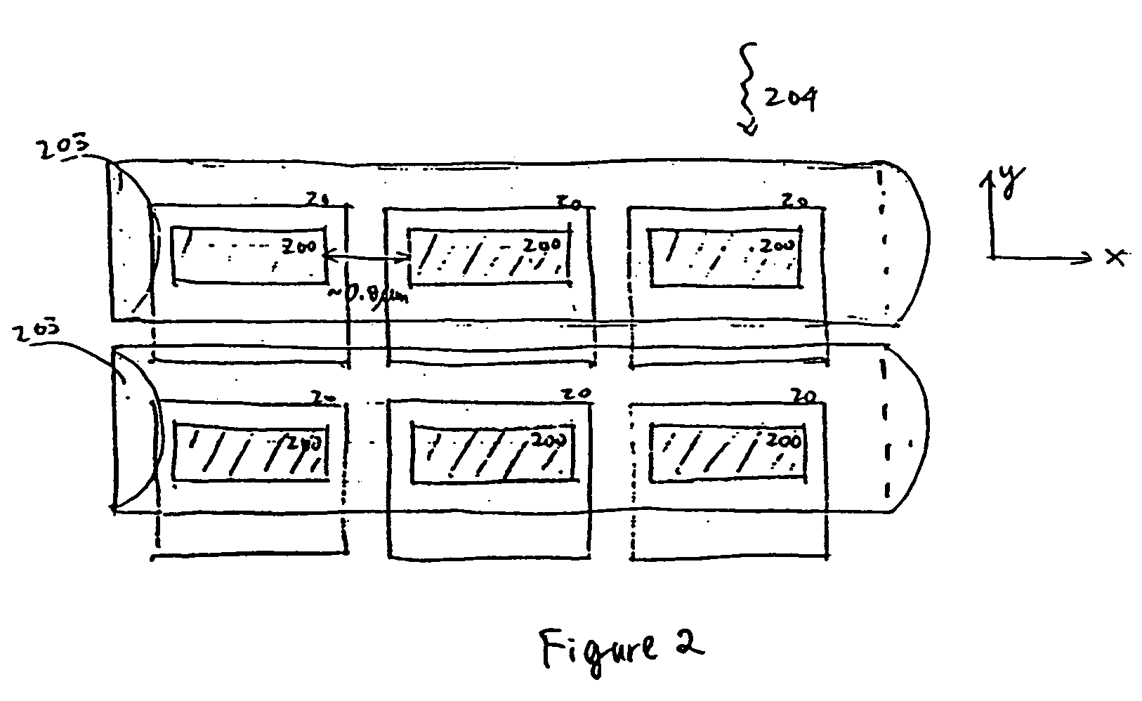
[0025] Unlike the rectangular-shaped image sensing area 100 of the unit pixel 10 for the CMOS image sensor of FIG. 1, the image sensing area 300 of the embodiment of FIG. 3, is square-shaped. And, as shown in the exemplary embodiment of FIG. 4, the image sensing areas 400 for an array 40 of unit pixels 30, have an area of, for example, about 8×8 μm2. The spacing between neighboring image sensing areas 400 is, for example, around 4 μm, which is an improvement in separation of approximately 3.2 μm compared to the spacing between neighboring pixels using rectangularly-shaped image sensi...
PUM
 Abstract
Description
Claims
Application Information