

Method and apparatus for manufacturing magnetoresistive element
- Summary
- Abstract
- Description
- Claims
- Application Information
AI Technical Summary
Problems solved by technology
Method used
Image

Examples
example 1
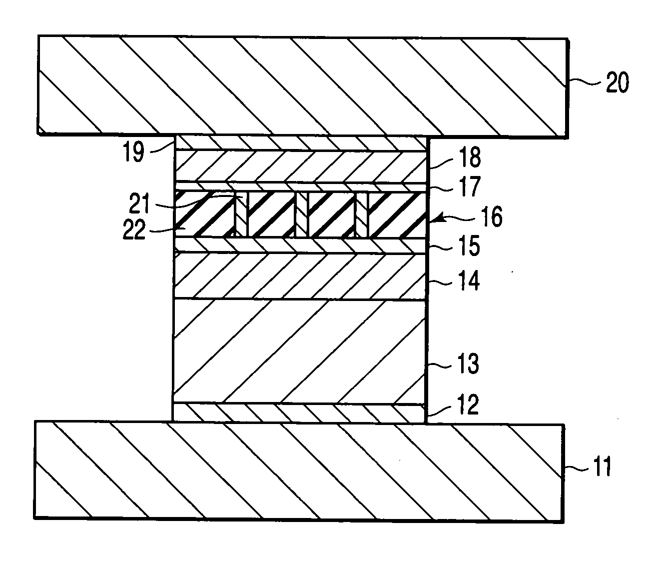
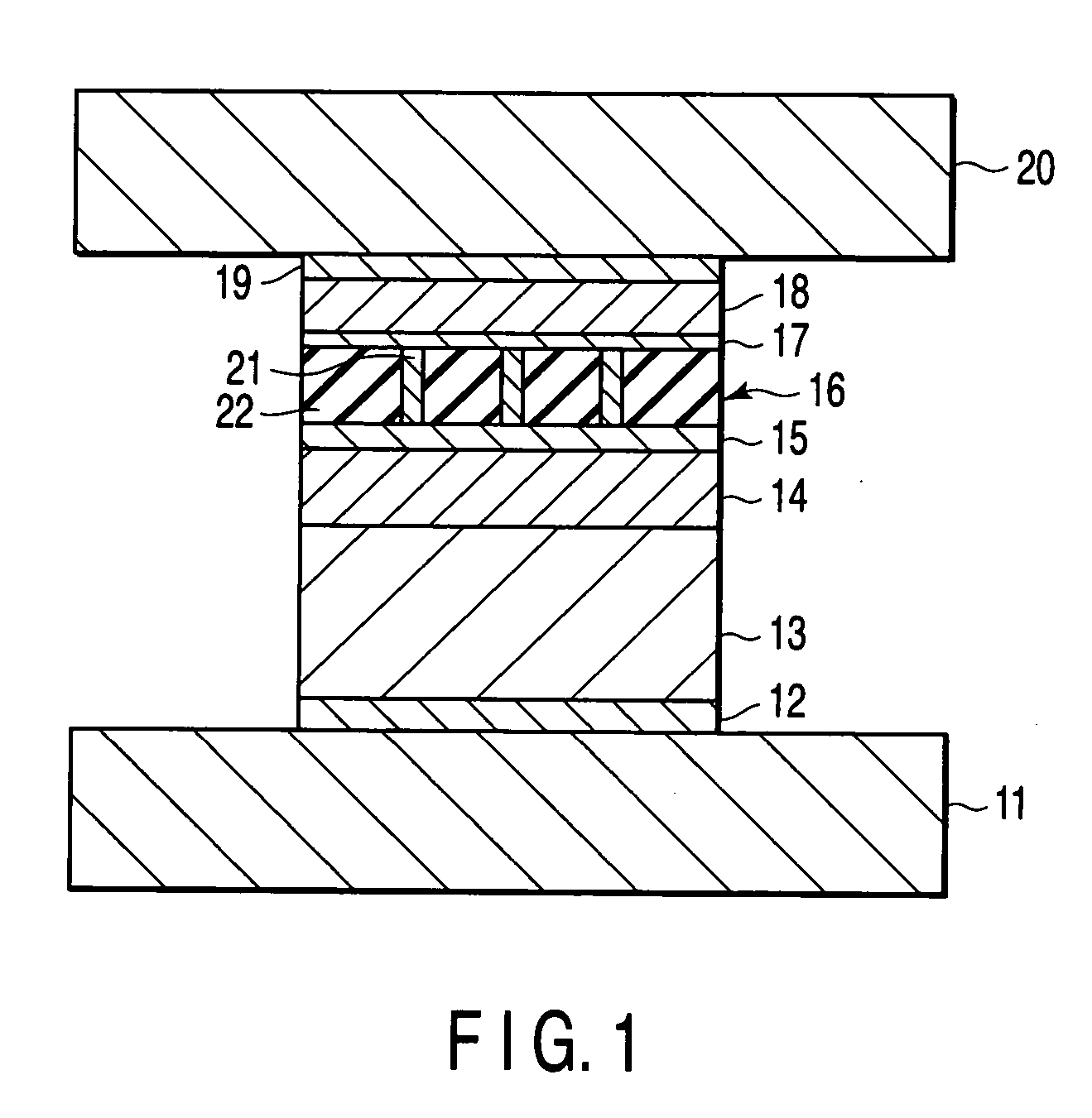
[0071]FIG. 6 is a perspective view of a magnetoresistive element (CCP-CPP element) manufactured in the present example. The magnetoresistive element shown in FIG. 6 has a structure in which the films listed below are sequentially stacked on a substrate (not shown):
[0072] lower electrode 11,
[0073] underlayer 12: Ta [5 nm] / Ru [2 nm],
[0074] pinning layer 13: Pt50Mn50 [15 nm],
[0075] pinned layer 14: Co90Fe10 [3.6 nm] / Ru [0.9 nm] / (Fe50Co50 [1 nm] / Cu [0.25 nm])×2 / Fe50Co50 [1 nm],
[0076] metal layer 15: Cu [0.5 nm],
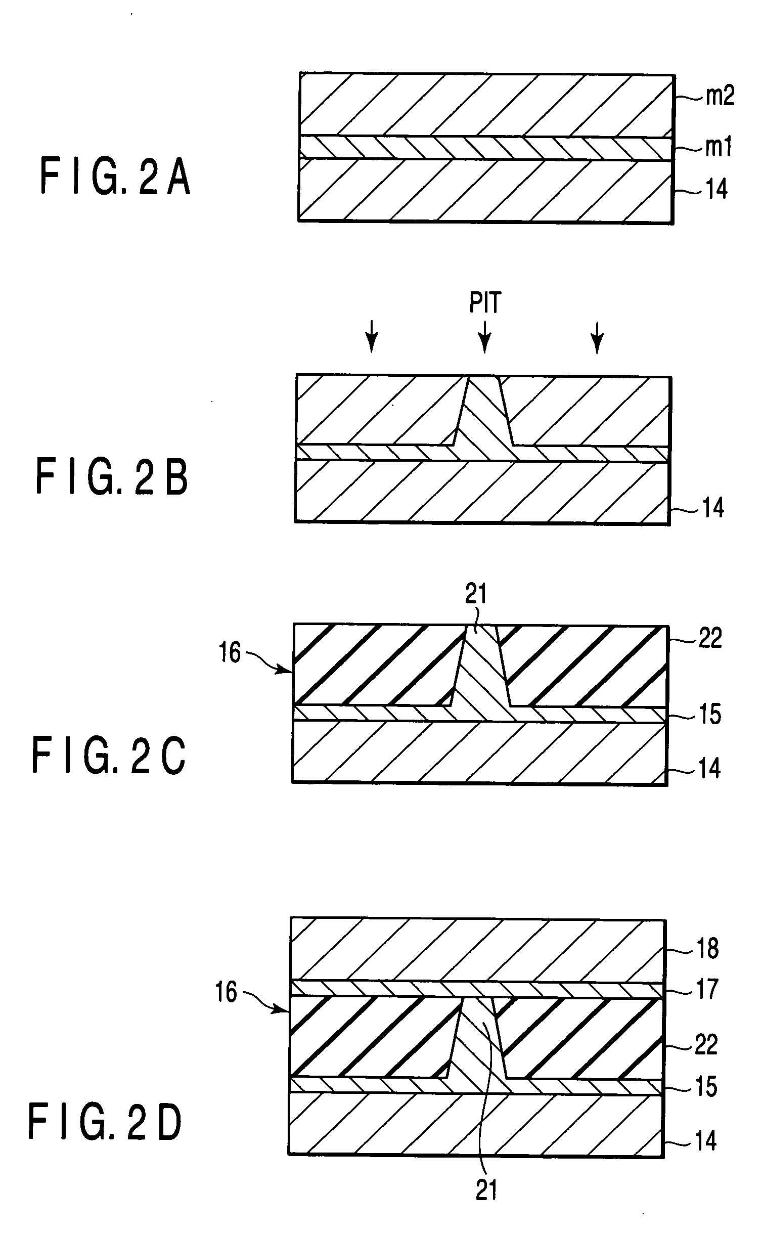
[0077] spacer layer (CCP-NOL) 16: Al2O3 insulating layer 22 and Cu current paths 21 (prepared by depositing Al90Cu10 [1 nm], followed by performing PIT and IAO treatment),
[0078] metal layer 17: Cu [0.25 nm],
[0079] free layer 18: Co90Fe10 [1 nm] / Ni83Fe17 [3.5 nm],
[0080] cap layer 19: Cu [1 nm] / Ru [10 nm], and
[0081] upper electrode 20.
[0082] In the description below, the spacer 16 and the metal layers 15 and 17, disposed over and under the spacer layer 16, may be collect...
example 2
[0110] Comparison between the characteristics of CCP-CPP elements produced by various methods will be described. The materials for the layers from the underlayer 12 to the cap layer 19 are listed below:
[0111] underlayer 12: Ta [5 nm] / Ru [2 nm],
[0112] pinning layer 13: Pt50Mn50 [15 nm],
[0113] pinned layer 14: Co90Fe10 [4 nm] / Ru [0.9 nm] / Co90Fe10 [4 nm],
[0114] metal layer 15: Cu [2.5 nm],
[0115] spacer layer (CCP-NOL) 16: Al2O3 insulating layer and Cu current paths 21 (prepared by depositing Al90Cu10 [x nm], followed by performing PIT and IAO treatment),
[0116] metal layer 17: Cu [2.5 nm],
[0117] free layer 18: Co90Fe10 [1 nm] / Ni83Fe17 [3.5 nm],
[0118] cap layer 19: Cu [1 nm] / Ru [10 nm].
[0119] In the present example, the thickness x of AlCu, used as a second metal layer, was varied between 0.5 and 1 nm. To vary the thickness of AlCu corresponds to vary the area ratio of the current paths in the CCP-NOL surface, and thus, this enables to adjust RA of the CCP-CPP element. That is, ...
example 3
[0141] In the present Example, materials advantageous for achieving a high MR ratio in a CCP-CPP element manufactured by the method according to the present invention will be described. Specifically, Co90Fe10 or Fe50Co50 was used as a material for the magnetic layers provided over and under the spacer layer. The layers in the CCP-CPP element from the underlayer to the cap layer are as follows:
[0142] underlayer: Ta [5 nm] / Ru [2 nm],
[0143] pinning layer: PtMn [15 nm],
[0144] pinned layer: Co90Fe10 [4 nm] / Ru [0.9 nm] / “Mag” [4 nm],
[0145] metal layer: Cu [2.5 nm],
[0146] spacer layer: Al2O3 insulating layer and Cu current paths 21 (prepared by depositing Al90Cu10 [x nm], followed by performing PIT and IAO treatment),
[0147] metal layer: Cu [2.5 nm], and
[0148] free layer: “Mag” [4 nm].
[0149] In the present example, Co90Fe10 or Fe50Co50 was used as a magnetic layer denoted as “Mag”. FIG. 12 shows evaluations of the characteristics of these CCP-CPP elements. FIG. 12 also shows the resu...
PUM
 Abstract
Description
Claims
Application Information