

Precision surface treatments using dense fluids and a plasma
Inactive Publication Date: 2004-01-08
JACKSON DAVID P
View PDF9 Cites 196 Cited by
- Summary
- Abstract
- Description
- Claims
- Application Information
AI Technical Summary
Benefits of technology
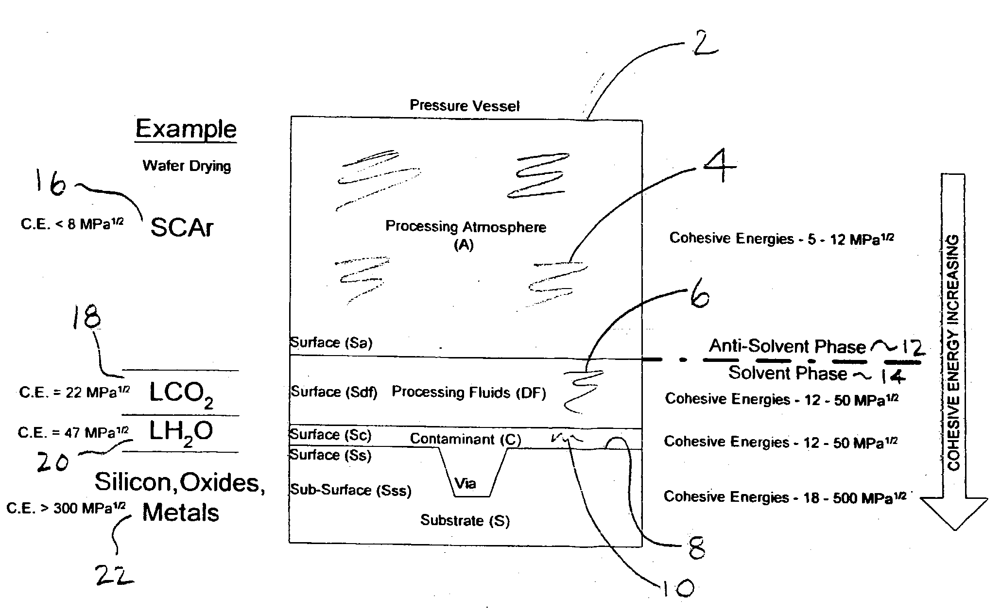
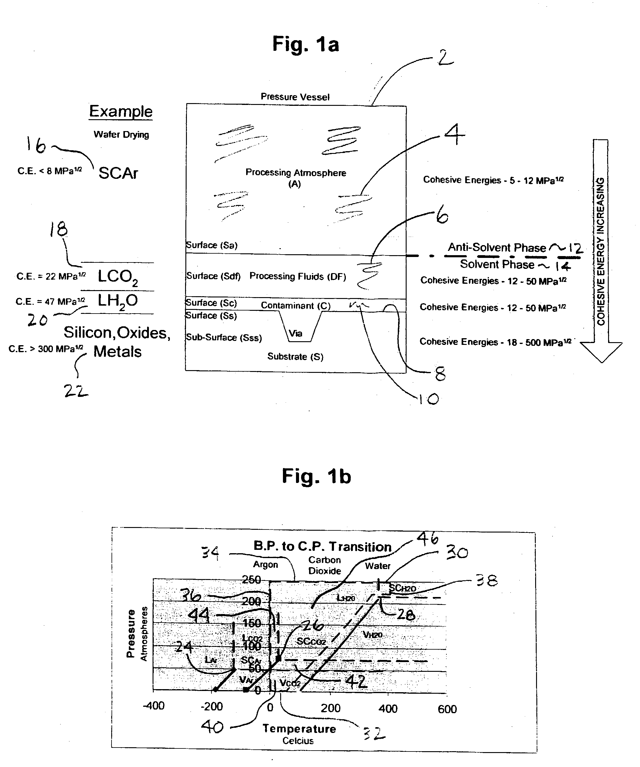
[0120] A particular advantage of the present invention as opposed to prior art is the application of a relatively small quantity of dense fluid (solvent) to the topside surface of a rotating substrate within an established and substantially inert (anti-solvent) supercritical nitrogen (or other suitable dense gas anti-solvent) environment. For example, dense fluid solvents chosen for the present invention have higher densities, and very divergent cohesion energies, than the dense fluid anti-solvents. Because of the differences in dielectric properties between and overall poor thermal conductivities of the dense fluids chosen for the present invention, the processing environment can be segregated into distinct zones which have different properties and are used to control certain aspects of the exemplary treatment processes described herein.
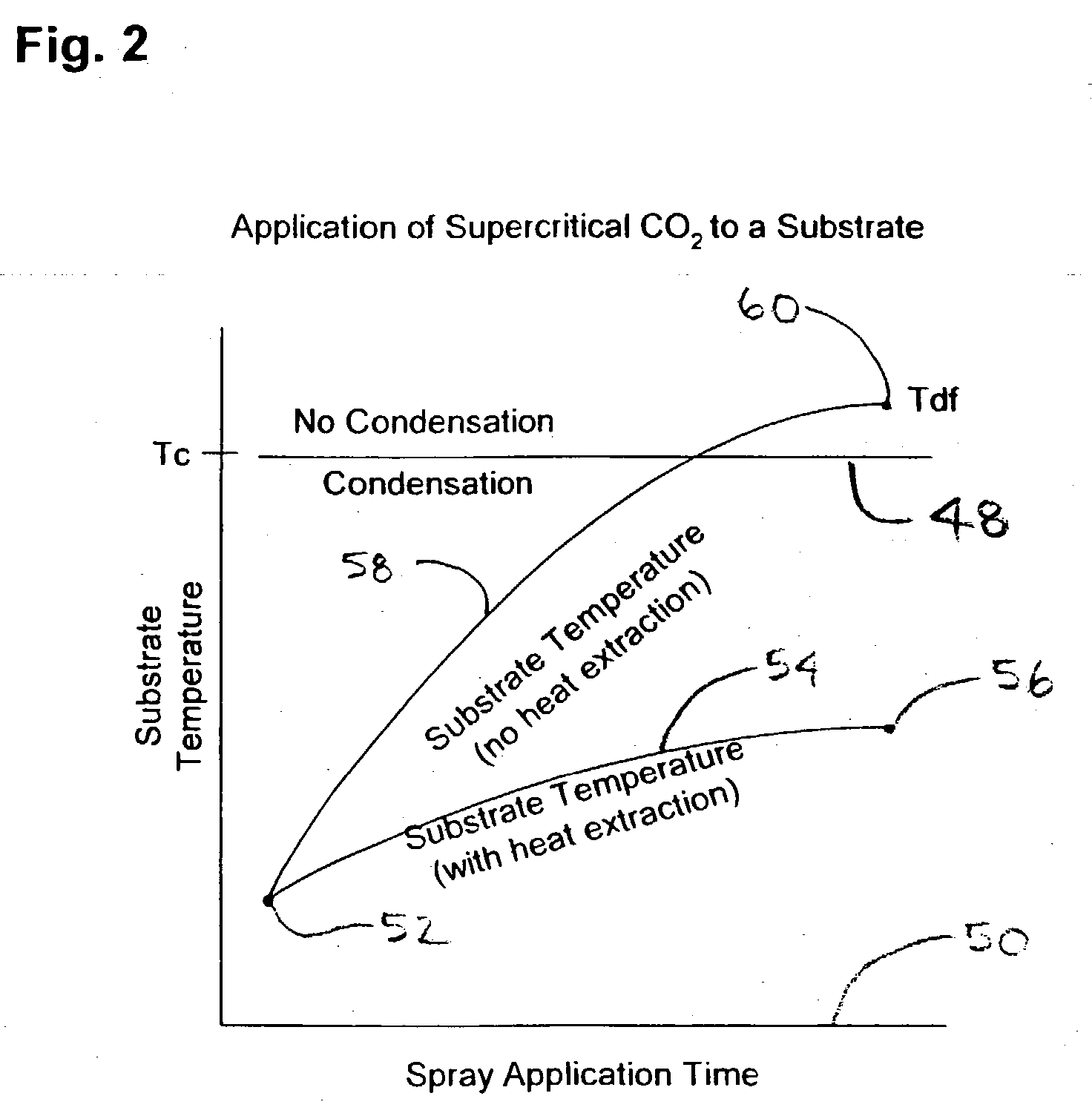
[0121] For example, selectively applying heat energy to an upper portion or zone of the antisolvent atmosphere (Ta), where Ta>Tdf, and extracting heat from the lower portion or zone of the anti-solvent atmosphere (T<Tscf), the supercritical carbon dioxide may be selectively condensed to a liquid-phase within a lower hemisphere of the process chamber and collected simultaneously during the application of the supercritical fluid spray to the substrate surface above. Due to the poor thermal conductivity between the anti-solvent phase and solvent phases of the present invention, a temperature gradient can be established in the process chamber under relatively constant pressure. Thus, a thermal gradient and a constant pressure (isobaric) process condition can be maintained within the chamber and between a dense fluid supply tank during processing. An anti-solvent supercritical fluid zone is established above and surrounding the substrate to selectively alter the interfacial physicochemistry (change cohesion energy or change phase) of a dense fluid solvent spray and substrate surface.
[0122] In addition, and simultaneously with the application of the supercritical fluid solvent, a lower temperature zone may be established below the substrate surface to collect reacted dense fluid as a `condensed phase`, which separates readily within the process chamber due to both density and cohesive energy increases. Thus, another advantage of the present invention is that a variety of dense fluid solvent pressures, temperatures and conditions can be applied to and reacted with the surface of a substrate under isobaric conditions and using pulsation, gravity flow, or high pressure spray techniques. Moreover, another advantage of the present invention is that the process chamber does contain a significant quantity of liquefied dense fluid phase carbon dioxide or other spent dense fluid solvent at any given time. Contaminants, water and particles contained within a hemisphere below a substrate and in a very small quantity of dense fluid relative to the volume of the process chamber are much less likely to become entrained within the anti-solvent phase due to significant differences in cohesion energy, density, and viscosity. Therefore the use of a condensed-phase zone as taught herein serves as a liquid trap for reaction by-products and prevents re-deposition of contaminants onto substrate surfaces above.
[0123] In another aspect of the present invention, a substrate is plasma cleaned in a supercritical argon atmosphere at a temperature which is below the critical temperature and greater than the critical pressure of carbon dioxide. Under these conditions, the substrate is rotated in a clockwise or counterclockwise direction. The impingement spray, in this case liquid carbon dioxide, is introduced at a pressure that is equal to or greater than the internal anti-solvent atmosphere. In fact, the dense fluid spray pressure and temperature can be applied at much greater pressure than the internal pressure of the anti-solvent atmosphere. During application of the dense fluid jet spray, a high voltage high frequency showerhead electrode is energized. The supercritical argon and liquid carbon dioxide acts as a dielectric barrier fluid, through which a uniform plasma discharge is created. The presence of oxygen (carbon dioxide is a source of oxygen) in the dense fluid fluid flow over the substrate results in the generation of oxygen radicals and supercritical ozone which serve as powerful surface cleaning adjuncts.
[0124] Moreover, plasma adjuncts of the present invention may be used under sub-atmospheric and atmospheric conditions which provides a capability producing clean or etched substrates using combinational cleaning under different pressure, temperature, fluid conditions and with different gaseous and liquid admixtures. This capability allows the operator to develop any variety of highly selective substrate treatment processes incorporating cold and thermal plasma treatments with liquid and supercritical phase dense fluid treatments. Still moreover, plasma-aided deposition processes may be developed with the dense fluid cleaning treatments.
[0125] Process variables for the present invention include, among others, dense fluid solvent spray pressure, temperature, and flowrate, substrate rotational velocity, and supercritical fluid anti-solvent pressure, chemistry (type of gas or mixture), pressure and temperature, and electric field strength (plasma density). These variables must be optimized for each type of substrate treated and for each type of treatment process developed--for example a "dry-clean-deposit" or a "clean-etch-clean" treatment combination. For example, it may be optimal to slowly flow supercritical carbon dioxide containing a deposition compound over a cold substrate (e.g. 15 C.) which is rotated at a low angular velocity (e.g. 10 rpm) to produce a desired coating thickness. In another example, it may be optimal to spray a substrate with high pressure liquid carbon dioxide over a superheated substrate (e.g. 100 C.) rotating at very high angular velocity (e.g. 2000 rpm) to remove tenacious surface contaminants.
Problems solved by technology
Smaller circuits and surface features are becoming increasingly affected by smaller surface particles and other residues (contaminations) during manufacturing operations.
Moreover, many conventional wet cleaning techniques are not compatible with the shrinking device geometries and new manufacturing materials.
The presence of organic contaminants or particles on a substrate surface with thicknesses on the order of 0.1 microns or greater generate considerable cleaning difficulties.
The trend towards miniaturization of silicon, germanium and gallium arsenide microprocessors in the electronics industry and the emergence of new microelectromechanical systems (MEMS) manufacturing, which uses much the same microprocessor manufacturing technology, is creating new material and process challenges.
For example, the smaller dimensions create new cleaning challenges due to increasing capillary force pressures which hold process fluids within cavities, more prevalent electrostatic forces which hold micromechanical structures together, porous or complex surface topography which preclude the use of aqueous chemistries, and high aspect ratio cavities and vias which hide etch residues and particles, among others.
Moreover, new materials such as low-k films and copper lines used to fabricate smaller device geometries (line widths) are not compatible with many conventional wet processing techniques described above.
However, the compliant nature of the silicon makes it susceptible to fabrication problems.
A significant problem in the fabrication of the micromachined components is sticking of released structures to the substrate after they are dried using conventional air drying techniques.
Electrostatic forces due to electrostatic charging may cause sticking.
This is a non-equilibrium condition which usually dissipates over time or with contact between conducting surfaces.
Second, a smooth surface finish may cause stiction.
The impurities in narrow gaps formed by the suspended microstructures essentially bridge the gaps, causing the structures to stick.
Perhaps the most troublesome cause of surface stiction is liquid bridging.
Interfacial forces generated when the trapped capillary fluid dries can cause the microstructures to collapse and stick.
Moreover, conventional thermal or solvent drying of silicon IC structures such as microvias cause the cavity walls to crack as the sidewalls are pulled together during extraction or evaporation of water or high surface tension drying solvents such as methyl alcohol.
If a liquid such as water is present in small capillaries during the drying process, the surface tension exerts tremendous pressure on the sidewalls.
This stress can be high enough to cause smoothe flat interfaces to stick, or in the case of IC fabrication, microvia sidewalls to collapse.
The most significant drawbacks with the aforementioned conventional dense fluid drying techniques are very long process cycle times and the use of excessive amounts of supercritical or liquid carbon dioxide in completely flooded pressure vessels to remove only trace amounts of surface contamination (i.e., water and drying solvents).
Another drawback is that these drying methods do not effectively remove small particles and in fact can easily re-contaminate substrates which are completely bathed in the reactor fluid.
Moreover, these methods are not effective or selective for removing other liquid contaminations present on the substrate surface or trapped within pores of substrates.
Still moreover, solid contaminants such as carbon residues are not effectively removed using these conventional techniques, even when modified with organic solvents.
Most often extreme pressures are required to achieve separation.
If left on critical surfaces, these may bridge circuits, obscure light or produce other deleterious side-effects which reduce yields, that is clean dry surfaces for subsequent processing steps.
Moreover, processes described above such as cleaning, etching, drying and application of coatings are most often performed as separate operations, which greatly increases the risk of device contamination during manufacture.
This system suffers from an inability to apply thermal energy to the substrate because it lowers the solubility of ozone in solution and is essentially time-dependent and concentration-dependent solid-ozone gas interfacial reaction.
However, similar to the DIO3 process, transport of ozone of any significant concentration into micron features on the wafer surface is very limited due to the solid-ozone gas interface.
Moreover excessive agitation caused by rapid movement of water over the spinning wafer accelerates the decomposition of the ozone gas as it diffuses through the thin film boundary.
Moreover, complete drying of the substrate following cleaning by both methods is also limited due to hydration of small capillaries, vias and interstices present on the wafer.
This method is similar to ozonated water treatment of wafer and suffers from the same solubility and selectivity problems.
A limitation with this method is its inability to actually remove particles from the wafer.
In fact, the rapid deployment of water from the tank often transfers more particles onto the wafer.
In addition, the wafers from the quick dump tank must still undergo a drying operation, further increasing the number of particles on the wafer.
However, the spin rinse / dryer often introduces more particles onto the wafer.
Another limitation with the spin rinse / dryer is its complex mechanical design with moving parts and the like.
The complex mechanical design often leads to problems such as greater downtime, wafer breakage, more spare parts, and increased cost of ownership, among other issues.
A further limitation is static electricity often builds up on the wafers during the spin cycle, thereby attracting even more particles onto the surface of the semiconductor.
Accordingly, the spin rinse / drying does not clean or remove particles from the wafer.
This superheated or saturated drying vapor often requires the use of large quantities of a hot volatile organic material.
A limitation with this type of dryer is its use of the large solvent quantity, which is hot, highly flammable, and extremely hazardous to health and the environment.
Another limitation with such a dryer is its cost, which is often quite expensive.
However, hot water often produces stains on the wafer, and also promotes build-up of bacterial and other particles.
However, '936 does not teach first establishing an inert supercritical fluid atmosphere into which a liquefied gas or supercritical fluid such as carbon dioxide may be much more selectively applied and controlled.
Moreover, the '936 method as well as very similar prior art by the present inventor, for example U.S. Pat. No. 5,368,171, and practiced commercially since about 1992 by Deflex Corporation using a commercial centrifugal liquid carbon dioxide spray cleaning device (Deflex SuperFuge.TM.) suffer from an inability to fully exploit the delivery agent (dense fluid) chemistry, as the liquid-state carbon dioxide chemistry is not a variable geometry dense fluid.
This is a significant disadvantage as elevated temperatures improve spray cleaning performance, lowering particle adhesion and increasing contaminant solubility, and increases the solubility of high molecular weight polymers such as photoresist resins.
For example, in '936 the liquid phase carbon dioxide surface tension, density and viscosity cannot be varied to any significant degree, which prevents optimization of solute chemistry and substrate cleaning and deposition processes.
Moreover, the substrate is contained in the saturated dense fluid vapor atmosphere which requires large quantities of dense fluid and extra processing steps to remove.
Using this method, most of the cleaning fluid is wasted and cross contamination problems arise.
The process of '366 is inefficient because it changes the properties of an entire fluid environment to process a substrate surface.
Also '366 will not remove small surface particles because it does not produce sufficient shear stress energy during the phase transition.
The process of '366 is inefficient because it changes the properties of an entire fluid environment to process a substrate surface--causing the coating to coat all surfaces of the reactor and substrate simultaneously.
Moreover, the prior art does not propose the novel and beneficial aspects of combining plasmas with dense fluids.
Plasma cleaning processes are widely used to remove patterned photoresist, however radiation damage to MOS circuits can be a problem as well as an inability to remove carbon-fluorine sidewall contaminants produced by deep reactive ion etching (RIE) processes.
Though this can be advantageous for organic removal from ion sensitive components it also produces a less homogeneous process resulting in the compromising of uniformity across the work area.
In surface modification the effective depth of the modification is tens of nanometers so the uniformity of the process becomes increasingly important, rendering MW source plasmas a less desirable choice.
A major problem that prevents adequate adhesion is the presence of organic contamination on the surface.
The reaction is by its nature complete with no residual surface products, however non-organics such as salts are not so readily removed.
Lower power densities not only remove contamination at a slower rate but also can actually impede the removal process.
Large irregular surfaces also can be treated with little possibility of over-treatment, a drawback of both flame and corona methods.
Even the best stainless steel has been known to oxidize in a plasma environment and over time the oxidized surface can be a source of undesirable particulate.
Thus, it has a tendency to adsorb particulate and organic contamination from the ambient environment.
Particulate contamination will generally create unacceptable defects.
This may lead to non-uniform coatings, in particular if deposited from liquid media.
Surfaces can never be perfectly clean in ambient air.
Crosslinking of thick films of organic contaminants such as oils will hinder cleaning action because it creates a barrier (i.e., carbon) to subsequent plasma reactions.
However, high pressure plasma processing (i.e., P>1 atm) is still a relatively unexploited area.
Dense fluid plasma technology enables new surface treatment possibilities not possible using either technology alone.
If the rotation velocity is in a range, that the atmospheric friction leads to high Reynolds numbers (turbulences), disturbances in the coating quality are observed.
The water left absorbed on such surfaces and edges often attracts and introduces more particles onto the semiconductor wafer and is a outgas and adhesion contamination in subsequent photoresist deposition following cleaning and drying operations.
The aforementioned conventional techniques fail to provide such desired features, thereby reducing the die yield on the semiconductor following optical printing or lithographic processes.
Method used
View moreImage
Smart ImageViewing Examples

Examples
example 1
[0300] Precision cleaning a semiconductor wafer to remove submicron particles from microscopic structures using a condensing flow of supercritical carbon dioxide.
example 2
[0301] Precision drying a semiconductor silicone device containing optical switches to remove trace moisture and residues from microscopic interfaces using a plasma and liquid carbon dioxide spray.
example 3
[0302] Precision cleaning a silicon semiconductor wafer containing integrated circuits to remove post-plasma reactive ion etch residues (carbon-fluorine compounds) from sidewalls of microscopic vias using combinations of argon-oxygen plasma and a condensing spray of supercritical carbon dioxide.
Login to View More PUM
| Property | Measurement | Unit |
|---|---|---|
| Power | aaaaa | aaaaa |
| Power | aaaaa | aaaaa |
| Electric potential / voltage | aaaaa | aaaaa |
Abstract
The present invention is a method, process and apparatus for selective cleaning, drying, and modifying substrate surfaces and depositing thin films thereon using a dense phase gas solvent and admixtures within a first created supercritical fluid antisolvent. Dense fluids are used in combination with sub-atmospheric, atmospheric and super-atmospheric plasma adjuncts (cold and thermal plasmas) to enhance substrate surface cleaning, modification, precision drying and deposition processes herein. Moreover, conventional wet cleaning agents such as hydrofluoric acid and ammonium fluoride may be used with the present invention to perform substrate pre-treatments prior to precision drying and cleaning treatments described herein. Finally, dense fluid such as solid phase carbon dioxide and argon may be used as a follow-on treatment or in combination with plasmas to further treat a substrate surface.
Description
[0001] This invention claims the benefit, under Title 35, United States Code 119 (e), of Provisional Application No. 60 / 365,788, filed Mar. 21, 2002 entitled "Precision surface treatments using dense fluids and a plasma" which is hereby incorporated by this reference.BACKGROUND OF INVENTION[0002] Smaller electronic, optical and micromechanical devices, with nano-scale device manufacturing already on the horizon, are driving the need for improved cleaning and drying technology. Smaller circuits and surface features are becoming increasingly affected by smaller surface particles and other residues (contaminations) during manufacturing operations. Moreover, many conventional wet cleaning techniques are not compatible with the shrinking device geometries and new manufacturing materials. Still moreover, the transition to larger wafer substrates such as the 300 mm platform is driving the need for increased performance and productivity in cleaning and drying processes and tools. Precision ...
Claims
Login to View More Application Information
Patent Timeline
 IPC IPC(8): B08B7/00C23C16/02C23G5/00H01L21/306H01L21/312H01L21/316H01L21/768
CPCB08B7/0021H01L21/76829B08B2203/005C23C16/0227C23G5/00H01J37/3244H01J2237/335H01L21/02052H01L21/312H01L21/3121H01L21/31612H01L21/7682H01L21/76825H01L21/76826H01L21/76828B08B7/0035H01L21/76814H01L21/02274H01L21/02216H01L21/02164
InventorJACKSON, DAVID P.
OwnerJACKSON DAVID P