[0015] A comprehensive scrub operation is included in a
flash memory system to compensate for disturbs of storage levels in one group of memory cells that are caused by
programming, reading or erasing operations performed on another group of memory cells on the same
integrated circuit chip. The potential for such data disturbs increases as the
memory cell arrays shrink in size. There is a tendency, in order to save space, for various
signal lines to be shared among groups of memory cells such that one group of memory cells experiences potentially repetitive
exposure to voltages and / or currents during
programming, reading or erasing the memory cells of another group. By scrubbing the data stored in all groups of memory cells in an organized and continuous manner, corruption of stored data over time is significantly reduced. Also, the storage of an increased number of bits per memory
cell with an increased number of smaller
voltage threshold state ranges is made practical when the disturbed charge levels are corrected by methodically restoring them to their intended levels.
[0017] The scrubbing operation may be made adaptive to the integrity of the data read. For example, if one or a threshold level of data errors is found in one region of the memory
cell array, the rate of scrubbing in that region may be increased. Conversely, if no errors or only a few data errors less than a threshold are found in a given region, this allows lowering the rate of scrubbing of the given region. The frequency and location of scrub may also be adapted to usage levels and other
system parameters. These and other features of scrub are calculated to provide a balance between the need to maintain
data integrity and the need to maintain a high level of system performance. Scrub operations not likely to improve
data integrity are particularly avoided.
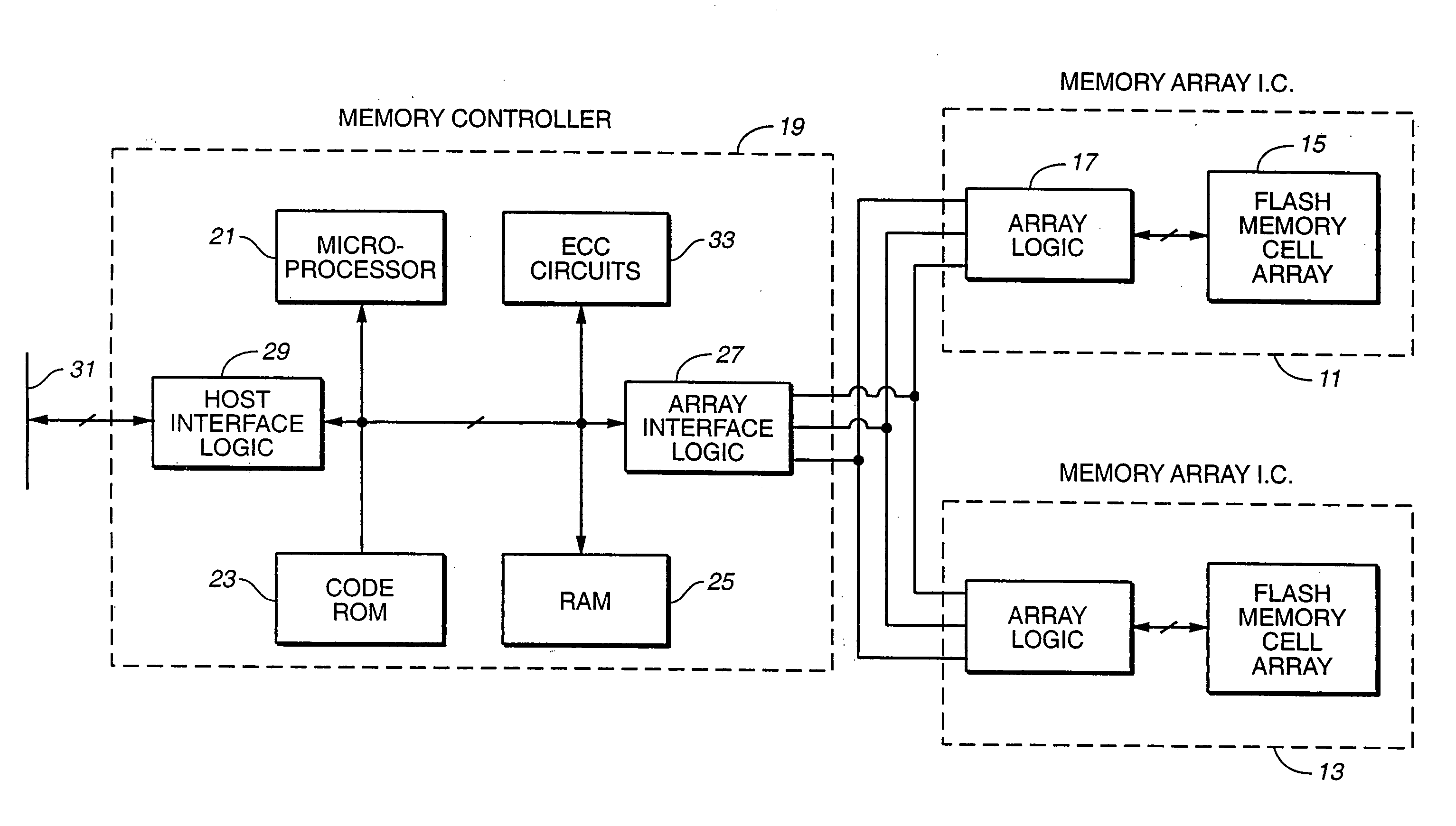
[0021] In
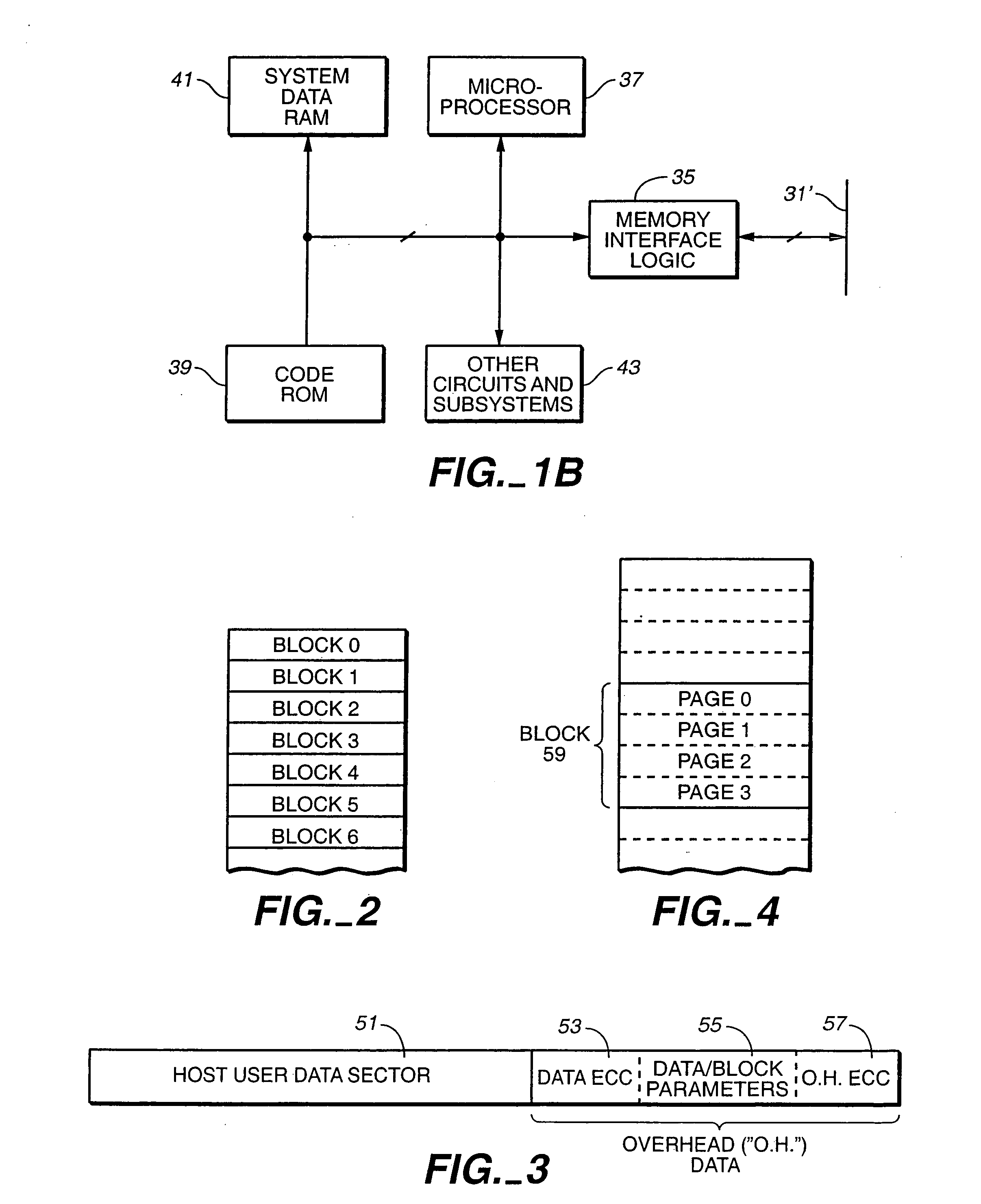
memory systems utilizing large blocks or metablocks of memory cells that individually store a large number of host data sectors, a sector(s) of data of a first physical block that are corrected during a scrub operation may be re-written into a second block into which remaining data sectors of the first block are copied, consistent with the erase
pooling method of
memory management described above. Alternately, a block or metablock may be dedicated to the
temporary storage of scrub corrected data sectors until other data sectors from the same blocks or metablocks as the corrected sector(s) need to be moved for some other reason, such as for
garbage collection, at which time the scrub corrected data sectors may be recombined with other data sectors of the same block or metablock. This improves system performance.
[0022] Once it is determined that corrective action needs to be taken with certain specified data, that action may be deferred if taking the corrective action at that time may adversely affect system performance, and if the data can be read without the corrective action, if necessary, before the corrective action later takes place. All corrected data, addresses and various parameters as determined at the time of deferral are temporarily stored and later retrieved when a deferred corrective action is executed. In systems organized in large blocks or metablocks of memory cells, corrective scrub actions may be deferred until a given amount of data from a given block or metablock are scheduled for corrective action, in which case all the deferred data sectors of the given block or metablock are corrected at the same time. This can reduce the amount of data
copying and re-writing that occurs when the data sectors of the given block or metablock are consolidated together again.
[0024] In addition to correcting data during scrub operations, sometimes data is corrected when the data is found to contain severe errors during a normal read operation. Severe errors are those that require immediate correction and
copying to a new location. Read operations usually have time constraints, so that data must be returned to a host within a
time limit. This
time limit may prevent
copying a block of data when a severe error is encountered during a read operation. However, a portion of the block may be copied within the time limit. Typically, just the portion of data (sector, page or some other portion that is less than a block) that contains the severe error is copied and the remaining portion of the block is left uncopied. The corrected portion of data may be copied to a dedicated correction block. A dedicated correction block may contain portions of data from different blocks of the
memory array. Similar techniques may be used in any situation where data is to be corrected and copied within a time limit. Where copying all the data would exceed the time limit, only portions containing errors may be copied and this may be done within the time limit. Even where no time limit applies, such techniques may be used to increase speed of correction.

