Check patentability & draft patents in minutes with Patsnap Eureka AI!

Method of forming via structures and method of fabricating phase change memory devices incorporating such via structures

Active Publication Date: 2006-02-23
SAMSUNG ELECTRONICS CO LTD
View PDF13 Cites 53 Cited by
  • Summary
  • Abstract
  • Description
  • Claims
  • Application Information

AI Technical Summary

Benefits of technology

[0016] Example embodiments of the invention provide methods for forming via structures having an improved capability for forming reliable via plugs within fine via holes.
[0017] Other example embodiments of the invention provide methods for fabricating phase change memory devices in which the via plugs formed from a phase change material layer within a small via hole exhibit improved reliability.
[0018] Still other example embodiments of the invention provide methods for fabricating phase change memory devices that omit anisotropic etching of the a phase change material layer and thereby reduce degradation of the operating characteristics of the phase change memory device.

Problems solved by technology

One drawback associated with phase change memory devices is the relatively high write current values that are required in order to induce a detectable phase change in the phase change material.
Typically, however, the phase change material layer is deposited using a sputtering method that tends to exhibit relatively poor step coverage that tends to complicate with efforts to uniformly fill fine via holes with the phase change material layer.
This overhanging region increases the likelihood that defects such as voids may be created within the phase change material layer filling the via hole.
However, if the phase change material, for example an alloy containing germanium-antimony (sometimes referred to as stibium)-tellurium (GST), is volatile or otherwise overly susceptible to the CMP process, excessive amounts of the material can be removed during the CMP process.
During such an anisotropic etch process, however, the exposed side portions of the GST alloy layer may suffer varying degrees of etch damage.
In particular, as the size of the GST alloy layer pattern is decreased to improve the degree of integration of the phase change memory device, the GST alloy layer pattern tends to become more susceptible to etch damage, thereby increasing the likelihood that the operating characteristics of the phase change memory device may be degraded and reduce the process yield and / or reliability of the resulting memory devices.

Method used


Image

  • Method of forming via structures and method of fabricating phase change memory devices incorporating such via structures
  • Method of forming via structures and method of fabricating phase change memory devices incorporating such via structures
  • Method of forming via structures and method of fabricating phase change memory devices incorporating such via structures

Examples


Embodiment Construction

[0033] Example embodiments of the invention will now be described more fully hereinafter with reference to the accompanying drawings, in which certain example embodiments of the invention are illustrated. Those of ordinary skill in the art will also appreciate that a range of alternative configurations have been omitted simply to improve the clarity and reduce the number of drawings. Those of ordinary skill will also appreciate that certain of the various structural elements illustrated or described with respect to the example embodiments may be selectively and independently combined to create other via filling processes and semiconductor device fabrication processes and / or methods useful for manufacturing semiconductor devices without departing from the scope and spirit of this disclosure.

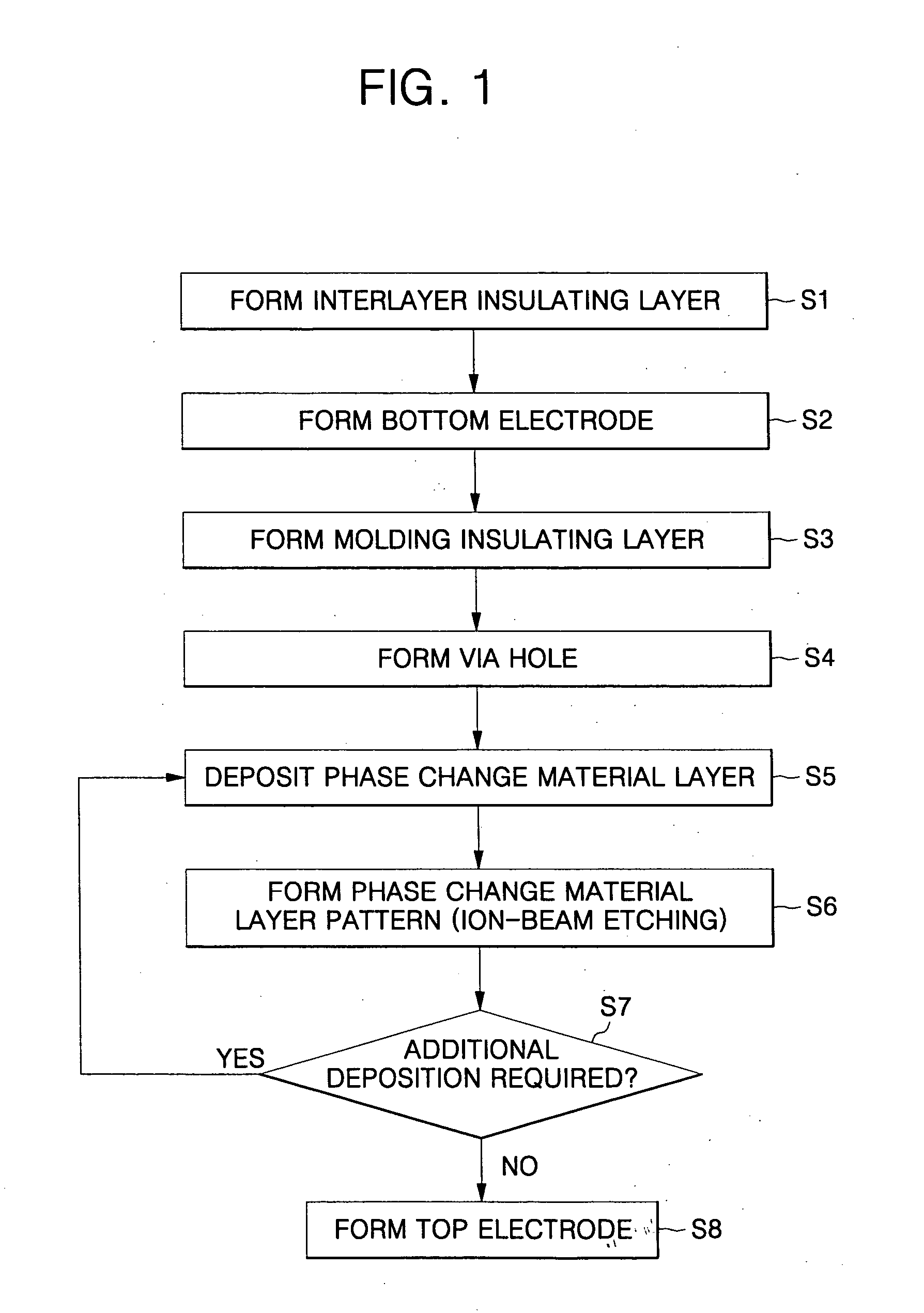
[0034]FIG. 1 is a process flow chart illustrating an example method of fabricating a phase change memory device in accordance with an example embodiment of the invention. In addition, FIGS. 2 to ...


PUM


Abstract

Provided are methods for forming conductive plug structures, such as via plugs, from a plurality of conductive layer patterns and methods of fabricating semiconductor devices, including semiconductor memory devices such as phase change semiconductor memory devices. An example method forms a small via structure by forming a conductive layer on a semiconductor substrate. A molding insulating layer is formed on the conductive layer and a via hole is formed through the insulating layer to expose a region of the conductive layer. A first via filling layer is formed and then partially removed to form a partial via plug. The formation and removal of the phase change material layer are then repeated as necessary to form a multilayer plug structure that substantially fills the via hole with the multilayer structure typically exhibiting reduced defects and damage than plug structures prepared by conventional methods.

Description

PRIORITY STATEMENT [0001] This application claims the benefit of Korean Patent Application No. 2004-66074, filed Aug. 20, 2004, the contents of which are hereby incorporated herein by reference in their entirety. BACKGROUND OF THE INVENTION [0002] 1. Field of the Invention [0003] The invention relates to example methods of fabricating semiconductor devices and, more particularly, to example methods of forming small via structures on a semiconductor device during the process of fabricating a phase change memory device. [0004] 2. Description of the Related Art [0005] Non-volatile memory devices share an ability to maintain stored data for a period of time even when the power supply to the memory device is interrupted. Accordingly, non-volatile memory devices are widely utilized computers, mobile communication systems, memory cards, and other applications in which the memory may be powered and accessed infrequently. [0006] Flash memory devices are a class of non-volatile memory devices...

Claims


Application Information

Patent Timeline
IPC IPC(8): H01L21/44
CPCH01L21/76877H01L45/06H01L45/1233H01L45/1683H01L45/143H01L45/144H01L45/126H10N70/8413H10N70/8825H10N70/231H10N70/066H10N70/8828H10N70/826H01L27/10H10B99/00
Inventor LEE, JANG-EUNCHO, SUNG-LAEPARK, JEONG-HEE
Owner SAMSUNG ELECTRONICS CO LTD
Features
  • R&D
  • Intellectual Property
  • Life Sciences
  • Materials
  • Tech Scout
  • Unparalleled Data Quality
  • Higher Quality Content
  • 60% Fewer Hallucinations
Learn More