SD/MMC cards

a technology of memory cards and mmc cards, applied in the direction of printed circuit aspects, electrical apparatus casings/cabinets/drawers, instruments, etc., can solve the problems of limiting the maximum height of the slot, the maximum thickness of the portion of the pda card contained within the slot, and the complexity of the pda card and the portable unit that uses it, etc., to achieve high density

Inactive Publication Date: 2006-03-02
SYCHIP
View PDF4 Cites 32 Cited by
  • Summary
  • Abstract
  • Description
  • Claims
  • Application Information

AI Technical Summary

Benefits of technology

[0011] We have designed a high density PDA integrated circuit card that overcomes in part the height constraint for IC components on the PDA card. We achieve this by building the printed circuit board platform on two levels. We have recognized that the contact pad end of the card should meet the 1.4 mm thickness maximum, while the remaining card portion is only constrained by the 2.1 mm thickness maximum. We take advantag...

Problems solved by technology

The complexity of the PDA cards and the portable units that use them increases as more functionality is added.
The combination of these circuits on a single PDA card presents a challenge for the PDA card designer.
The length×width maximums place severe co...

Method used


Image

  • SD/MMC cards
  • SD/MMC cards
  • SD/MMC cards

Examples


Embodiment Construction

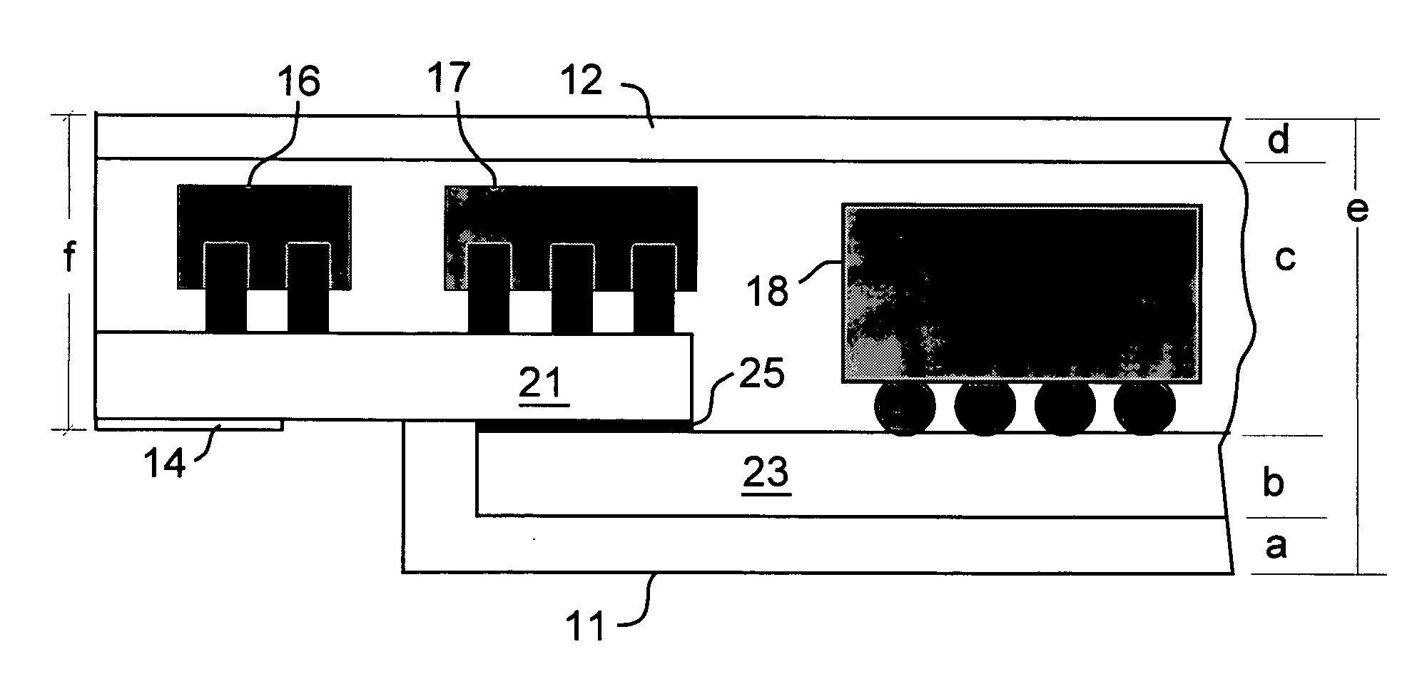
[0017] With reference to FIG. 1, a portion of a PDA card is shown with printed circuit board (PCB) 10, bottom plastic cover 11 and top plastic cover 12. The PDA card assembly is typically molded in a plastic encasement (usually the top and bottom covers), typically an epoxy or other tough polymer. Such encasements are well known in the art and widely used. Digital components and devices, such as capacitors, inductors, oscillators, filters, IC chips, etc., are mounted on the PCB. For devices with a wireless interface, for example an SDIO 802.11b card, the card will have relatively large RF ICs and devices.

[0018] In FIG. 1, three components, 16, 17, and 18 are shown by way of example. Typically there are many more components on the PCB 10, located on the portion not shown. They may be mounted in a variety of ways, for example, surface mount, flip-chip ball grid array (BGA), etc. Contact fingers 14 are shown along the edge of the PDA card, typically on an exposed portion of the PCB as...


PUM


Abstract

The specification describes PDA (SD/MMC) devices and PDA cards wherein the substrate on which the PDA components are mounted comprises two tiers. Components with a high profile are mounted on the lower tier, and devices with normal or low heights are mounted on the upper tier. The upper tier is contained in the portion of the card conforming to, for example, the 1.4 mm SDA standard thickness, while the lower tier is formed in the portion of the card that allows a larger thickness, for example SDA standard thickness 2.1 mm.

Description

FIELD OF THE INVENTION [0001] This invention relates to memory and interface cards for portable computer devices such as personal digital assistants, digital cameras, etc. More specifically it relates to Secure Digital (SD) or Multimedia Memory Card (MMC) type cards that meet existing size standards but have enhanced component packing density. BACKGROUND OF THE INVENTION [0002] (Portions of the technical material contained in this section may not be prior art.) [0003] The evolution of component miniaturization in computer technology now allows very small, portable, units that can be carried as personal items, for example, in briefcases, or clothing pockets. There are a variety of such devices available commercially. Among those well known in the trade are PDAs, personal PCs, digital cameras, cell phones, smart phones, etc. For convenience, these portable devices are generically referred to below as PDAs. However, the term should be recognized as referring to any portable electronic ...

Claims


Application Information

Patent Timeline
IPC IPC(8): H05K5/00H05K1/14
CPCG06K19/077H05K1/0284H05K1/0298H05K2201/09118H05K1/141H05K1/183H05K2201/09018H05K1/117G06K19/00
Inventor CHOU, WAI PINGSUN, KUNQUANWANG, JIAXIANYU, YANBINGZHAO, MENG
Owner SYCHIP
Why Eureka
Try Eureka