Mode-locked laser diode device and wavelength control method for mode-locked laser diode device

a laser diode and wavelength control technology, applied in the direction of laser details, semiconductor lasers, electrical apparatuses, etc., can solve the problems mechanical instability, and large and achieve the effect of increasing manufacturing costs, increasing manufacturing costs, and increasing the size of laser diodes

Inactive Publication Date: 2006-03-02
OKI ELECTRIC IND CO LTD
View PDF8 Cites 26 Cited by
  • Summary
  • Abstract
  • Description
  • Claims
  • Application Information

AI Technical Summary

Benefits of technology

[0052] According to the wavelength control method for the output optical pulses of the MLLD device described above, -the MLLD performs mode-locking operation in steps (A) and (B), and the CW light of which the intensity of the CW light is at a level where the effect of optical injection locking is sufficiently expressed and the mode-locking operation does not diminish, is input to the optical wave guide of the MLLD in steps (C), (D) and (E), so optical pulses, of which the wavelength width in the wavelength variable area is sufficiently wide and of which frequency chirping is suppressed, can be acquired.

Problems solved by technology

The problems of these optical pulse generation devices are that the sizes thereof are large and are mechanically unstable because of the large sizes.
In other words, the device is warped by the mechanical force, which fluctuates the time waveform shape of the optical pulse to be generated and cyclic frequency of the optical pulse, and this makes operation unstable.
The fluctuation of the time waveform of the optical pulse and cyclic frequency of the optical pulse to be generated can be prevented by feedback using a feedback circuit, but integrating such a feedback circuit into the device increases the manufacturing cost, and also increases the power consumption of the device.
In other words, in terms of practicality, constructing a mode-locked laser device using an optical fiber laser and external resonator type diode is a poor idea.
However handling an FP resonator type MLLD device is difficult since the frequency chirping of the optical pulses to be output cannot be suppressed, as described above, and this frequency chirping strongly depends on the driving conditions of the MLLD.
In any case, the FP resonator type MLLD device is not appropriate to be integrated into an optical communication system.
Since an external resonator type laser is used, it is difficult to implement compactness and to secure stability of operation.
Also using an external resonator type laser tends to cause various problems due to the positional deviation of the optical system, such as the change of mode-locking characteristics and the appearance of composite resonator modes caused by the change of the ambient temperature.
The change of the ambient temperature also tends to cause such problems as a deviation from the frequency tuning range due to the change of the rotation frequency of the optical resonator.
Since a gain switch type laser is used, suppressing the time jitter and the frequency chirping of optical pulses has limitations.

Method used


Image

  • Mode-locked laser diode device and wavelength control method for mode-locked laser diode device
  • Mode-locked laser diode device and wavelength control method for mode-locked laser diode device
  • Mode-locked laser diode device and wavelength control method for mode-locked laser diode device

Examples


first embodiment

[0068] (Configuration)

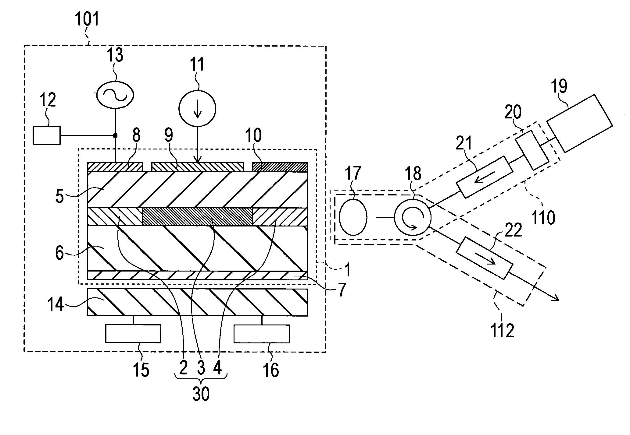
[0069] The configuration of the wavelength variable MLLD of the first embodiment of the present invention will be described with reference to FIG. 1. The MLLD device of the first embodiment comprises an MLLD 1, CW light source 19, first optical coupling means 110 and second optical coupling means 112. And the optical pulse generation section 101 is constructed including the MLLD 1.

[0070] The MLLD 1 further comprises an optical guide30 where the optical gain area 3, in which population inversion is created, and the optical modulation area 2 having a function to modulate the light intensity and passive wave-guiding area 4, are laid out in series, and this optical wave guide 30 propagates the oscillation light. The passive wave-guiding area 4 is made of transparent material which oscillation light of the MLLD 1 transmits through. In the first embodiment, the optical wave guide 30 created in the MLLD 1 is comprised of three areas: the optical gain area 3, optical...

second embodiment

[0136] (Configuration)

[0137] The configuration of the MLLD device according to the second embodiment of the present invention will now be described with reference to FIG. 8. The difference from the first embodiment is that the oscillation wavelength adjustment means is formed in the passive wave-guiding area 4. Specifically the oscillation wavelength adjustment means created in the passive wave-guiding area 4 is structured such that the current can be injected into the p-i-n junction created including the passive wave-guiding area 4 of the optical wave guide 30 by the second current source 23 via the p-side electrode 10 and the n-side common electrode 7. This p-i-n junction is created by the p-type clad layer 5, passive wave-guiding area 4 of the optical wave guide 30 which is the i-layer (intrinsic semiconductor layer) and n-type clad layer 6. In other words, the difference of this embodiment from the first embodiment is that the means for injecting current into the p-i-n junction...

third embodiment

[0160] (Configuration)

[0161] The configuration of the MLLD device according to the third embodiment of the present invention will now be described with reference to FIG. 11. The difference from the second embodiment is that the oscillation wavelength adjustment means is constructed such that the reverse bias voltage can be applied to the p-i-n junction comprised of the p-type clad layer 5, passive wave-guiding area 4 of the optical wave guide 30, which is the i-layer (intrinsic semiconductor layer) and n-type clad layer 6 by the reverse bias voltage source 24 via the p-side electrode 10 and the n-side common electrode 7. In other words, the difference of this embodiment from the first embodiment is that the means for applying the reverse bias voltage to the p-i-n junction is included. The rest of the configuration is the same as the MLLD device in the first embodiment, so redundant description is omitted for identical parts.

[0162] (Operation)

[0163] The MLLD device of the third em...


PUM


Abstract

The present invention generates optical pulses of which the wavelength width in the wavelength variable area is sufficiently wide and of which frequency chirping is suppressed enough to be used for optical communication systems.
The present invention is constructed by an optical pulse generation section 101 including MLLD1, CW light source 19, first optical coupling means 110 and second optical coupling means 112. An optical wave guide 30 which includes an optical gain area 3, optical modulation area 2 and a passive wave-guiding area 4 is created in the MLLD. Constant current is injected into the optical gain area from the first current source 11 via the p-side electrode 9 and the n-side common electrode 7. Reverse bias voltage is applied to the optical modulation area 2 by a voltage source 12 via the p-side electrode 8 and the n-side common electrode. The modulation voltage with a frequency obtained by multiplying the cyclic frequency of the resonator of the MLLD by a natural number is applied to the optical modulation area by a modulation voltage source 13. The output light of the CW light source is input to the optical wave guide of the MLLD via the first optical coupling means, and the output light of the MLLD is output to the outside via the second optical coupling means.

Description

BACKGROUND OF THE INVENTION [0001] 1. Field of the Invention [0002] The present invention relates to a mode-locked laser diode (MLLD) device and a wavelength control method for the MLLD device, for generating an ultra short optical pulse string having high repeat frequency using a mode-locking method. [0003] 2. Description of Related Art [0004] Ultra short optical pulse generation technology using a laser diode and optical fiber laser is attracting attention as an important technology for increasing the speed and capacity of optical fiber communication based on an optical time-division multiplex method. As the speed of optical fiber communication increases, an optical pulse light source which can generate optical pulses at a shorter cycle period is required. At the same time, the high quality of an optical pulse string to be generated, such as having suppressed frequency chirping and low phase noise, is also important for optical fiber communication. [0005] In the above description,...

Claims


Application Information

Patent Timeline
Patent Type & Authority Applications(United States)
IPC IPC(8): H01S3/098
CPCB82Y20/00H01S5/005H01S5/0064H01S5/024H01S5/4006H01S5/0265H01S5/06255H01S5/0657H01S5/34306H01S5/0261
Inventor ARAHIRA, SHIN
Owner OKI ELECTRIC IND CO LTD
Why Eureka
Try Eureka