Die package, conductive element, semiconductor device including same, microlens, system including same, and methods of manufacture

a semiconductor device and conductive element technology, applied in the field of semiconductor devices and components, can solve the problems of encapsulant filler particles becoming lodged between lead ends and underlying die surfaces, cracking or perforation of die coats, and non-uniform flow of encapsulant in conventional transfer molding within mold cavities, etc., to facilitate electrical connection

Active Publication Date: 2006-03-02
MICRON TECH INC
View PDF99 Cites 84 Cited by
  • Summary
  • Abstract
  • Description
  • Claims
  • Application Information

AI Technical Summary

Benefits of technology

[0021] In one aspect of the present invention, a plurality of semiconductor dice may be at least partially encapsulated or packaged by application of a flowable dielectric material thereabout and subsequent bulk or en masse hardening or curing thereof. More particularly, a plurality of semiconductor dice may be disposed upon a carrier and a package material, such as, for instance, a photopolymer, may be disposed about the periphery of the semiconductor dice and at least partially cured substantially en masse. The uncured material may be prevented from at least partially curing proximate to the contact or bond pads of the at least

Problems solved by technology

Undesirably, encapsulant flow during conventional transfer molding within mold cavities is demonstrably nonuniform.
Therefore, encapsulant filler particles may become lodged between lead ends and the underlying die surfaces because the flow characteristics of the viscous encapsulant flow may cause particles to be forcefully driven between the lead ends and the additional surfaces of the semiconductor die and wedged or jammed in place in low-clearance areas.
When mechanical, thermal or electrical stresses attendant to post-encapsulation processing are added to the residual stresses associated with the lodged filler particles, cracking or perforation of the die coat may occur.
It has been observed that filler particle-induced damage may occur more frequently in close proximity to the adhesive, where lead flexibility is relatively low.
In addition to damage by filler particles, transfer molding also results in the problem of bond wire sweep, wherein bond wires may be damaged, broken, or loosened from their connections to bond pads or lead ends, or swept into shorting contact with an adjacent bond wire under the impetus of the flow front of molten resin encapsulant as it flows through a mold cavity.
Also, due to increased pressures exerted on the encapsulant, a small amount

Method used


Image

  • Die package, conductive element, semiconductor device including same, microlens, system including same, and methods of manufacture
  • Die package, conductive element, semiconductor device including same, microlens, system including same, and methods of manufacture
  • Die package, conductive element, semiconductor device including same, microlens, system including same, and methods of manufacture

Examples


Embodiment Construction

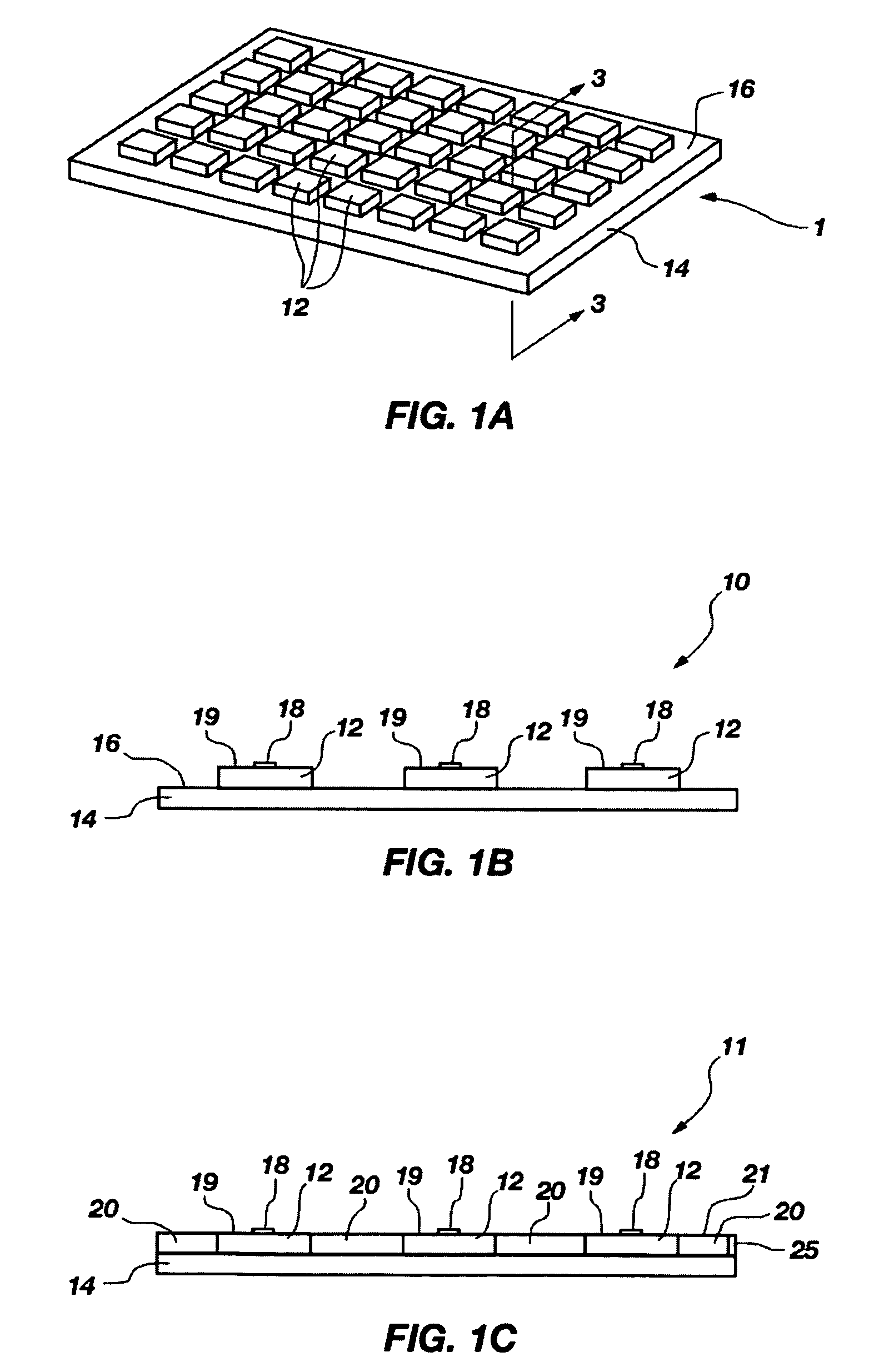
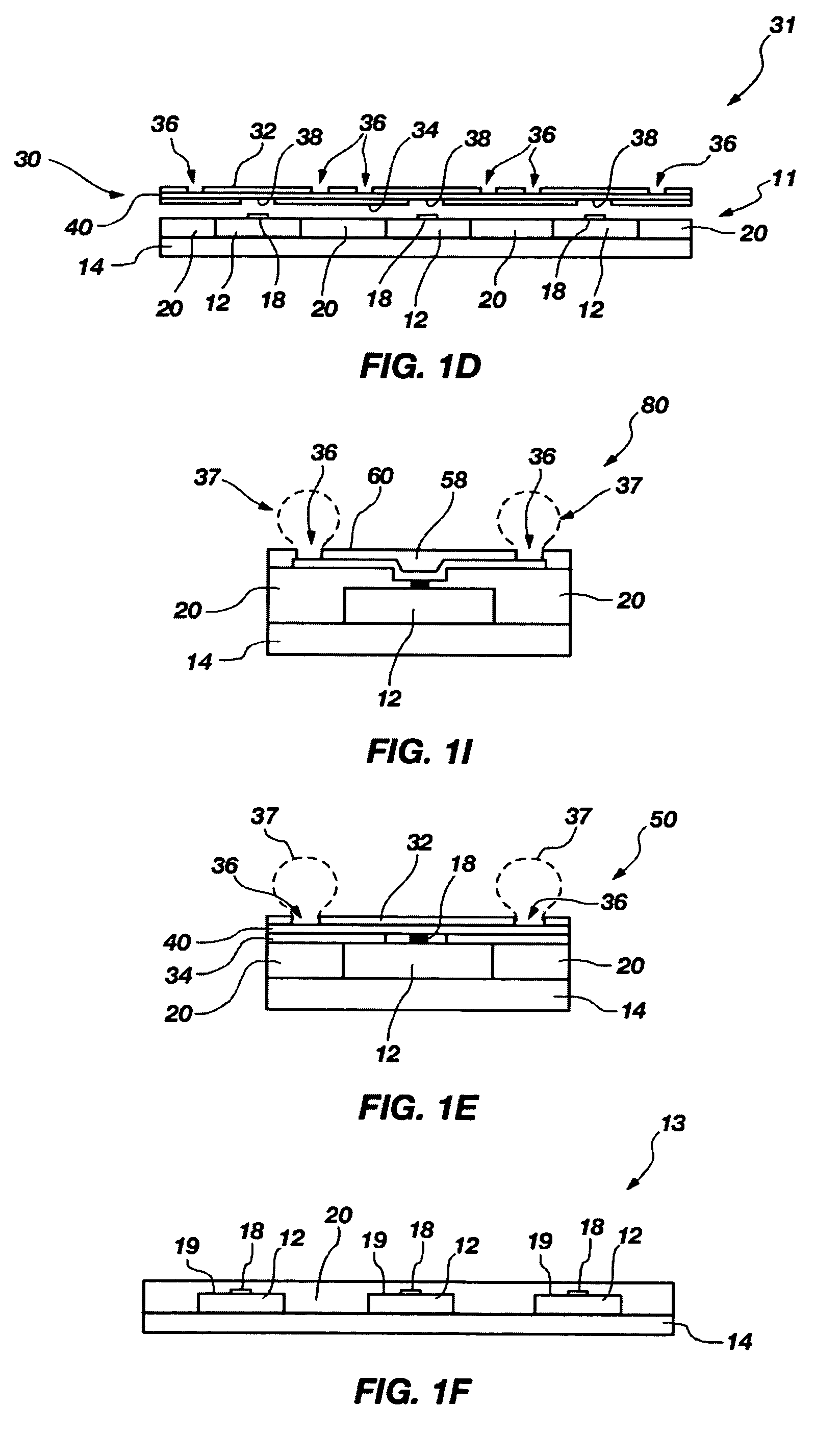
[0060] In one aspect of the present invention, one or more semiconductor dice may be at least partially encapsulated by application of a curable material thereabout and subsequent bulk or en masse hardening or curing thereof. More particularly, one or more semiconductor dice may be disposed upon a carrier and a package material (also termed an encapsulant), such as, for instance, a photopolymer, may be disposed about the periphery of the semiconductor dice and cured substantially in bulk or en masse. Subsequent to hardening or curing, the package material may be patterned, if necessary, to expose contact or bond pads of the semiconductor dice. Conductive traces and surface mount components may be disposed or formed as desired during or after the hardening of the package material. Such a configuration may eliminate the need for expensive transfer molding equipment and may provide increased flexibility in manufacturing.

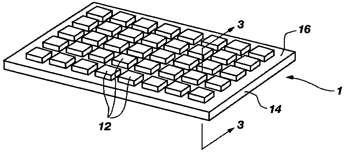
[0061]FIG. 1A shows, in a perspective view, array 10, which inclu...


PUM


Abstract

A method of packaging at least a portion of a semiconductor die or dice is disclosed. Uncured material may be disposed proximate at least the periphery of at least one semiconductor die and at least partially cured substantially as a whole. Method of forming conductive elements such as traces, vias, and bond pads are also disclosed. More specifically, forming at least one organometallic layer to a substrate surface and selectively heating at least a portion thereof is disclosed. Also, forming a layer of conductive photopolymer over at least a portion of a surface of a substrate and removing at least a portion thereof is disclosed. A microlens having a plurality of mutually adhered layers of cured, optically transmissive material, methods of forming same, and systems so equipped are disclosed.

Description

BACKGROUND OF THE INVENTION [0001] 1. Field of the Invention [0002] The present invention relates to semiconductor devices and components. Particularly, the present invention relates to at least partially packaging a semiconductor die or dice. The present invention also relates to forming conductive elements such as traces, vias, and bond pads. In addition, the present invention relates to a microlens for directing light toward a photosensor, methods of forming same, and systems so equipped. [0003] 2. Background of Related Art [0004] The invention pertains to a method for sealing and protecting at least the periphery of one or more semiconductor dice. When a semiconductor die is conductively attached to a carrier substrate, conventionally encapsulating the assembly is very desirable to enhance the mechanical bond between the die and the substrate and to mutually laterally electrically isolate adjacent electrical connections therebetween. More specifically, one common configuration f...

Claims


Application Information

Patent Timeline
IPC IPC(8): H01L21/50
CPCH01L21/56H01L23/3128H01L27/14618H01L27/14627H01L27/14685H01L2924/12041H01L2224/20H01L2924/01005H01L2924/01027H01L2924/01046H01L2224/04105B33Y10/00B33Y80/00
Inventor WOOD, ALAN G.FARNWORTH, WARREN M.WATKINS, CHARLES M.BENSON, PETER A.
Owner MICRON TECH INC
Why Eureka
Try Eureka