Critical dimension control for integrated circuits

a critical dimension and integrated circuit technology, applied in the direction of instruments, photomechanical devices, optics, etc., can solve the problems of poor performance of eventual devices, difficult to achieve using current technology, and difficulty in adjusting the cd and providing proper patterning for underlying substrates

Active Publication Date: 2006-03-02
MICRON TECH INC
View PDF12 Cites 55 Cited by
  • Summary
  • Abstract
  • Description
  • Claims
  • Application Information

AI Technical Summary

Benefits of technology

[0007] In another aspect of the invention, a method of etching a substrate is disclosed. The method comprises patterning a photoresist layer to form a plurality of original features. A pattern is formed with a plural...

Problems solved by technology

However, adjusting the CD and providing proper patterning for underlying substrates can be difficult when using only a photoresist soft mask.
Poor line edge roughness can lead to poor performance of the eventual d...

Method used


Image

  • Critical dimension control for integrated circuits
  • Critical dimension control for integrated circuits
  • Critical dimension control for integrated circuits

Examples


Embodiment Construction

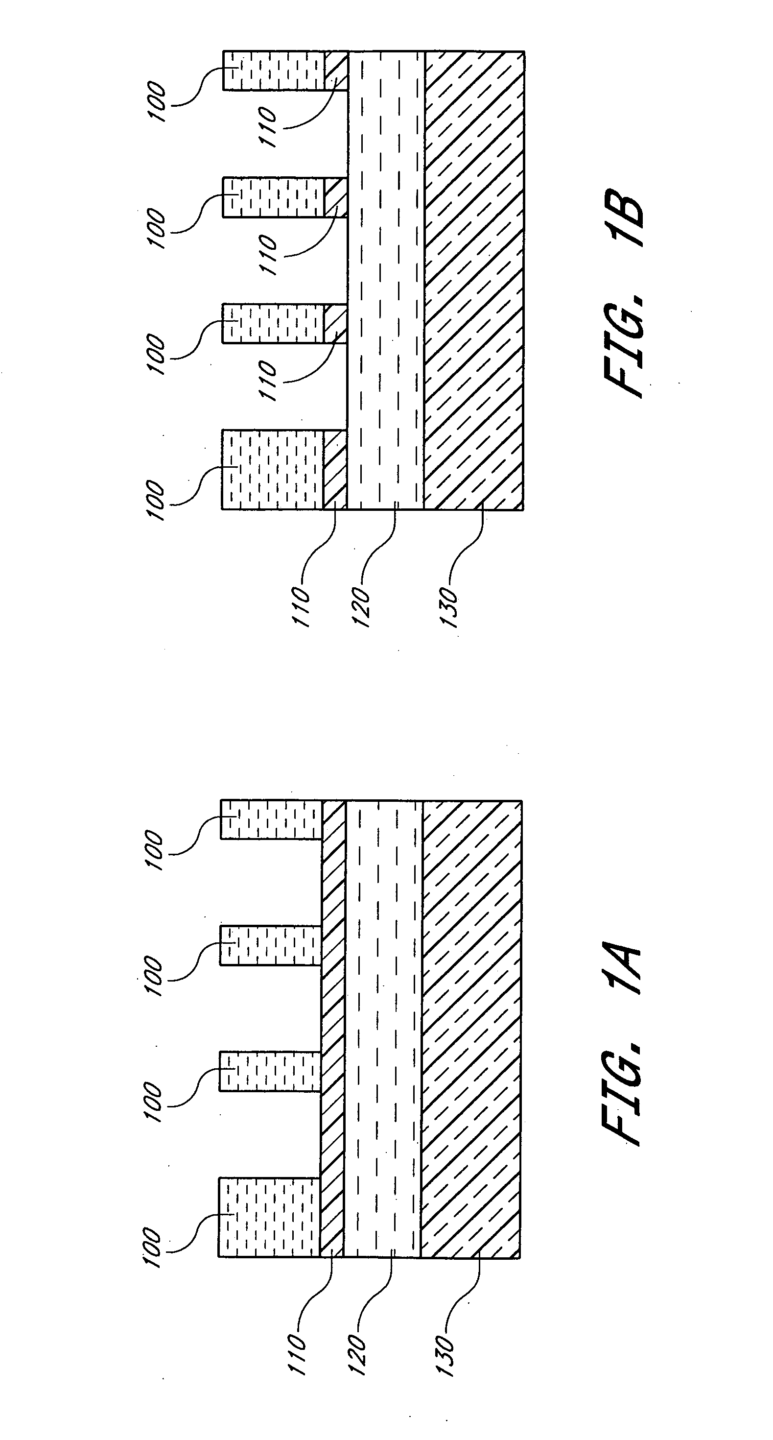
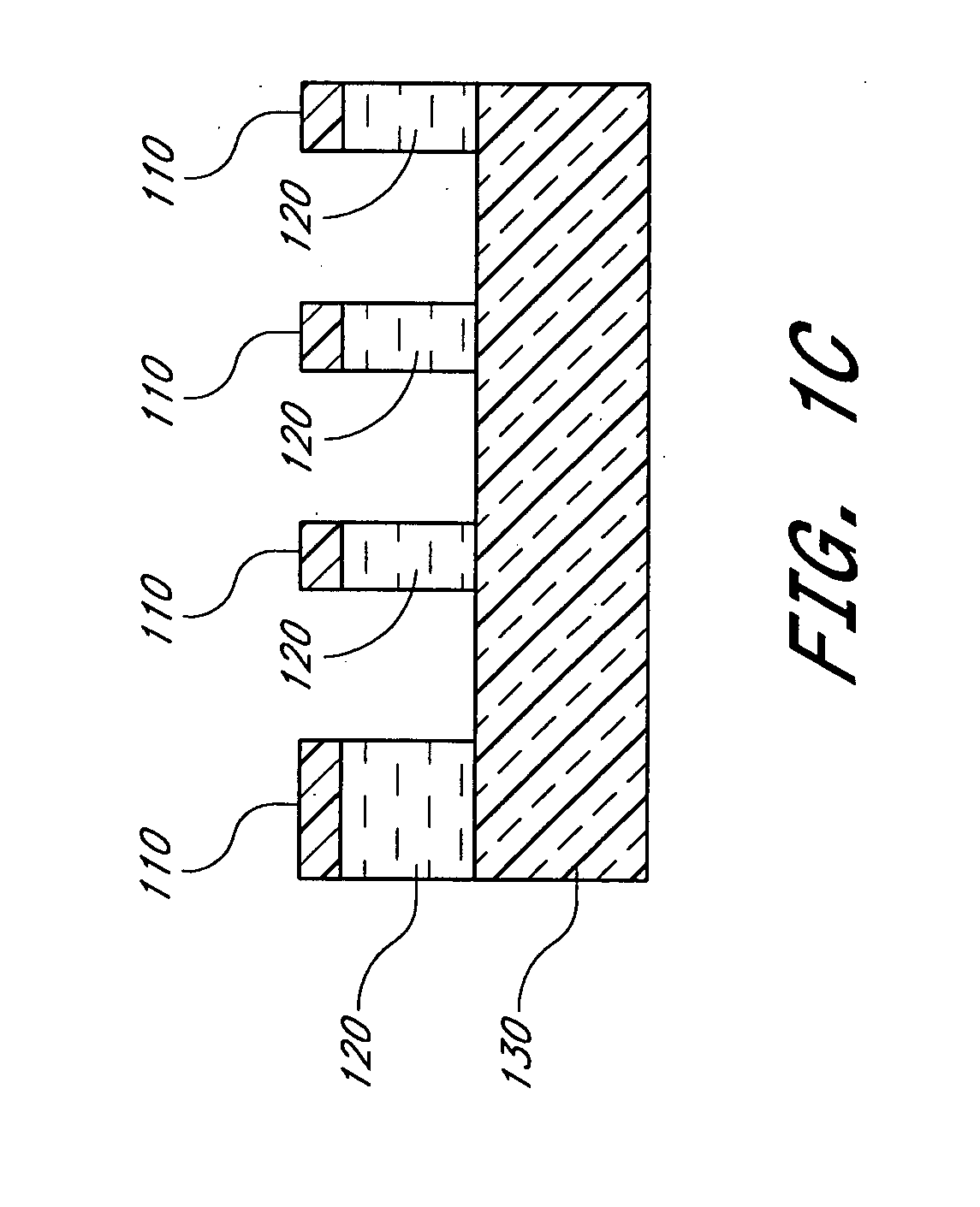
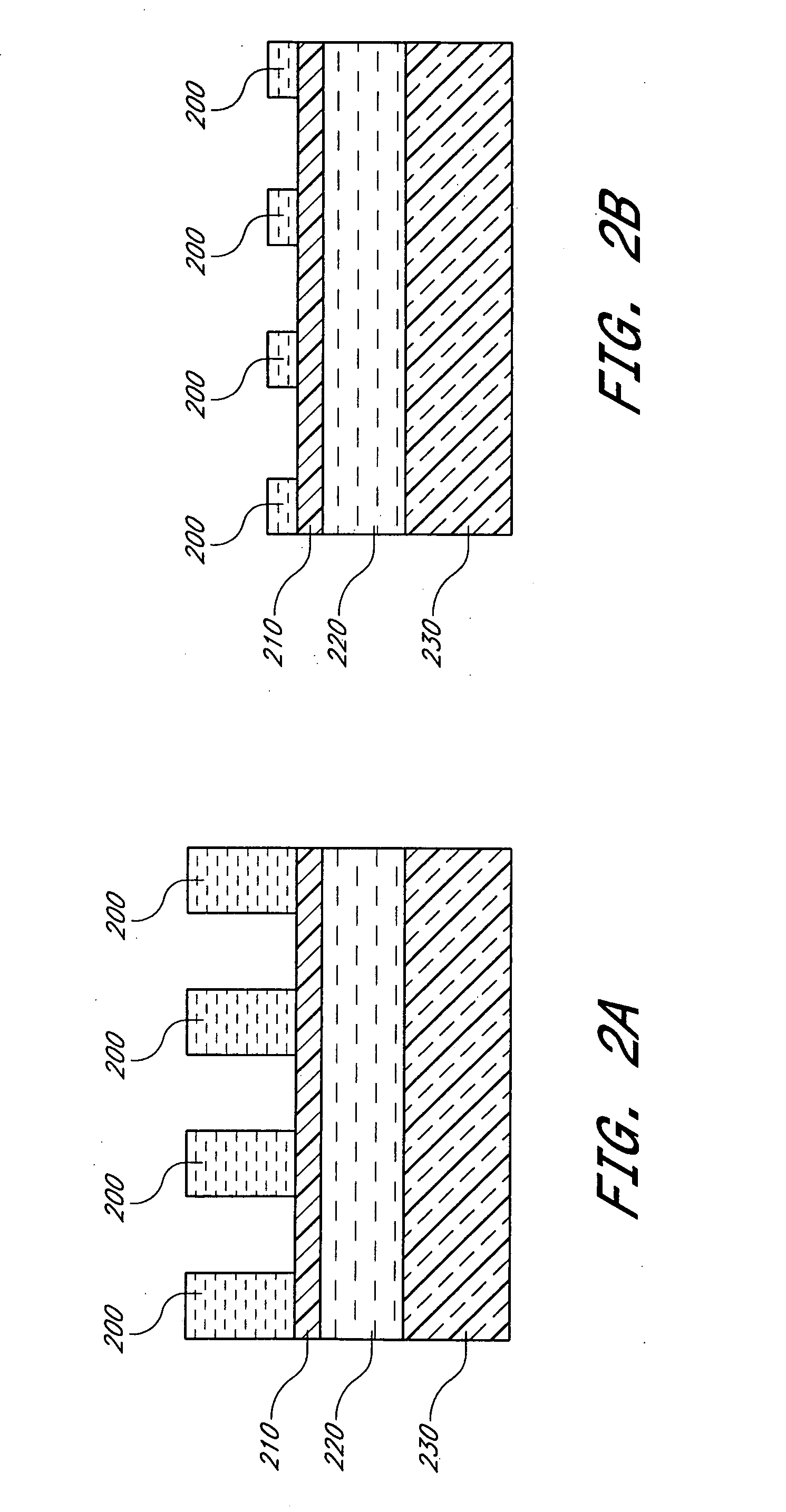
[0017] In the context of this document, the term “semiconductor substrate” is defined to mean any construction comprising semiconductor materials, including, but not limited to, bulk semiconductor materials such as a semiconductor wafer (either alone or in assemblies comprising other materials thereon), and semiconductor material layers (either alone or in assemblies comprising other materials). The term “substrate” refers to any supporting substrate, including, but not limited to, the semiconductor substrates described above. Also in the context of this document, the term “layer” encompasses both the singular and the plural unless otherwise indicated. As used herein, the term “organic” refers to carbon and carbon-containing materials, thus including amorphous carbon as well as photoresists. Also note that “sulfur oxide,” as used herein, means any compound consisting essentially of a combination of sulfur and oxygen, such as sulfur dioxide.

[0018] It will also be appreciated that tr...


PUM

PropertyMeasurementUnit
Poweraaaaaaaaaa
Poweraaaaaaaaaa
Poweraaaaaaaaaa

Abstract

Methods of etching substrates with small critical dimensions and altering the critical dimensions are disclosed. In one embodiment, a sulfur oxide based plasma is used to etch an amorphous carbon hard mask layer. The features of a pattern can be shrunk using a plasma etch to reduce the resist elements on the surface of the masking structure. Features in the pattern can also be enlarged by depositing polymer on the resist elements or by sloping an underlying layer. In one preferred embodiment, features of the pattern are shrunk before being enlarged in order to reduce line edge roughness.

Description

FIELD OF THE INVENTION [0001] The present invention relates to the field of integrated circuit fabrication, particularly to the etching process. BACKGROUND OF THE INVENTION [0002] Computer memory, like other integrated circuit (IC) devices, is getting faster, more cost-efficient, and more powerful. Dynamic Random Access Memory (DRAM) is a type of computer memory that stores information in memory cells, which typically comprise a transistor latched to a capacitor. [0003] The critical dimension (CD) is the dimension of the smallest geometrical features (width of interconnect line, contacts, trenches, etc.) which can be formed during semiconductor device manufacturing. Critical dimensions are shrinking in order to facilitate, the formation of smaller components and faster, more efficient circuits. However, adjusting the CD and providing proper patterning for underlying substrates can be difficult when using only a photoresist soft mask. [0004] Line edge roughness (LER) has tended to be...

Claims


Application Information

Patent Timeline
IPC IPC(8): H01L21/302
CPCH01L21/0331H01L21/0338H01L21/0337
Inventor ABATCHEV, MIRZAFER K.HWANG, DAVID K.VELTROP, ROBERT G.
Owner MICRON TECH INC
Why Eureka
Try Eureka