Multilayer wiring board and process for fabricating a multilayer wiring board

a multi-layer wiring and wiring board technology, applied in the direction of cable/conductor manufacturing, cross-talk/noise/interference reduction, conductive pattern formation, etc., can solve the problems of large space and investment for production, and large amount of materials used. , to achieve the effect of reducing the cost of apparatus, reducing the length of time required for forming the wiring pattern, and reducing the cost of equipmen

Inactive Publication Date: 2006-03-09
SONY CORP
View PDF3 Cites 11 Cited by
  • Summary
  • Abstract
  • Description
  • Claims
  • Application Information

AI Technical Summary

Benefits of technology

[0031] By virtue of having the above construction, in the process for fabricating a multilayer wiring board of the present invention, wiring patterns for all the layers can be formed on a single insulating sheet at the same time, and therefore not only can the length of time required for forming the wiring patterns be remarkably shortened, making the process suitable for the production of products of a number of types in respectively small amounts, but also only one apparatus is needed in the respective processing, making it possible to reduce the cost for apparatus.
[0032] By the multilayer wiring board and the process for fabricating a multilayer wiring board of the present invention, the length of time required for forming the wiring patterns can be remarkably shortened, and further the interlayer electrical connection with high reliability can be secured, and, in the multilayer wiring board containing an electronic part, an electromagnetic shielding structure which nullifies the effect of the electromagnetic interaction between the inside and the outside can be easily achieved, enabling a process suitable for the production of products of a number of types in respectively small amounts with a short lead time, and furthermore, only one apparatus is needed in the respective processing, thus making it possible to reduce the cost for apparatus.

Problems solved by technology

The fabrication process for a conventional multilayer printed wiring board is advantageously used in the mass production; however, a photomask is needed per layer in the exposure, and a pattern is formed per layer, and hence a prolonged preparation time is required, and there is a difference in yield between the layers formed, causing the amount of materials used to be large.
Specifically, a pattern is formed per layer and therefore, when the same apparatus is used, a production lead time is remarkably prolonged and, on the other hand, when parallel production is made, a plurality of apparatuses must be used, so that large space and investment for the production are required.
Further, the yields of formation of the patterns in the respective layers are likely to be different from one another, and therefore the amount of materials used is determined from the amount needed in the step having the lowest yield, so that materials in a large amount are inevitably used.
In this case, the case for electromagnetic shielding is placed on the printed wiring board and connected to the ground, and therefore there occurs disadvantages not only in that an additional operation of soldering is required, but also in that the case may be removed due to the vibration which the wiring board receives.
In this case, however, the conduction between the upper and lower flexible substrates stacked is achieved only through the stacked portions at the both ends of the flexible substrates, and therefore there is a problem in that a noise is generated or absorbed at any intermediate portion in the long wiring, causing the substrate to be sensitive to the electromagnetic interaction between the parts.

Method used


Image

  • Multilayer wiring board and process for fabricating a multilayer wiring board
  • Multilayer wiring board and process for fabricating a multilayer wiring board
  • Multilayer wiring board and process for fabricating a multilayer wiring board

Examples


Embodiment Construction

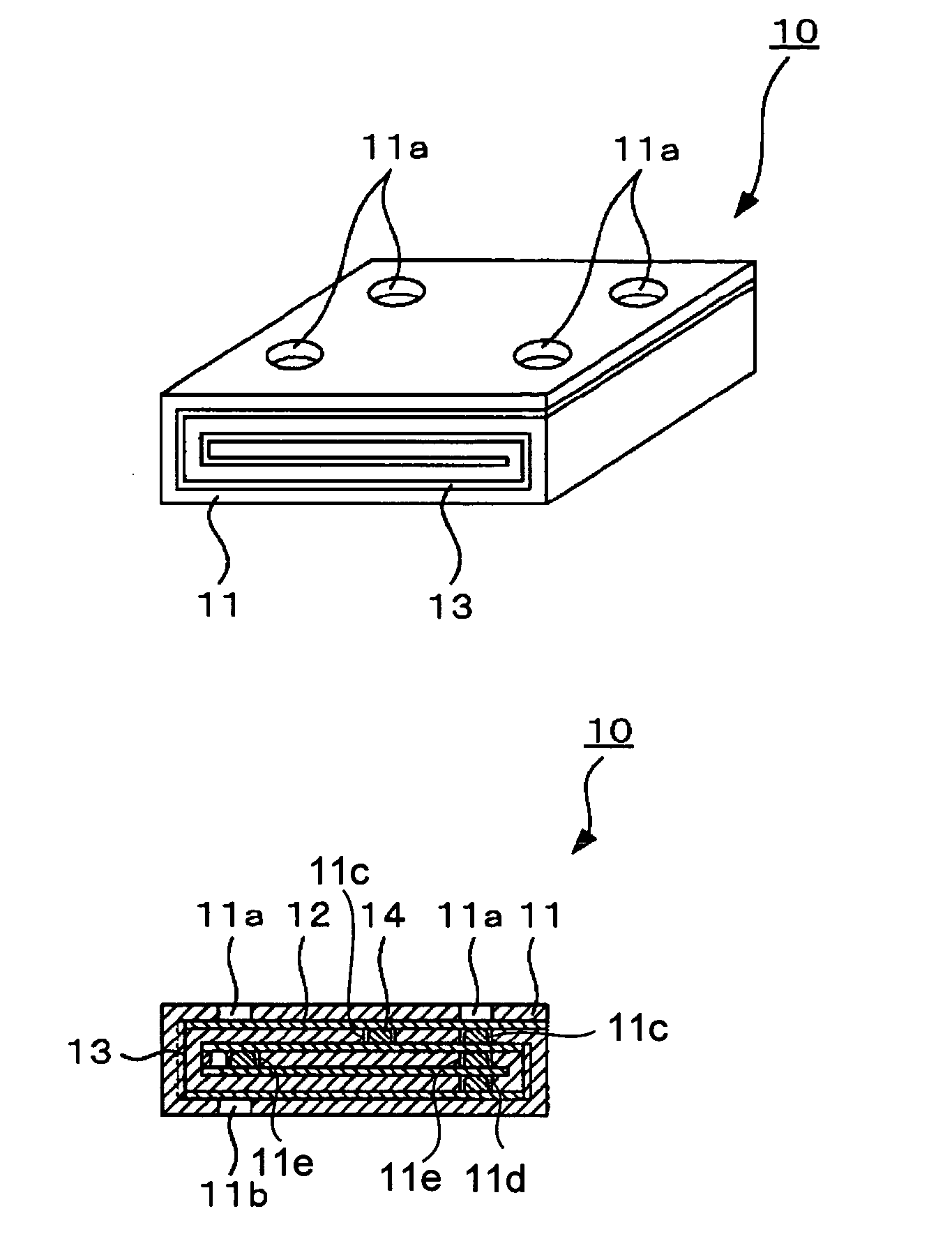
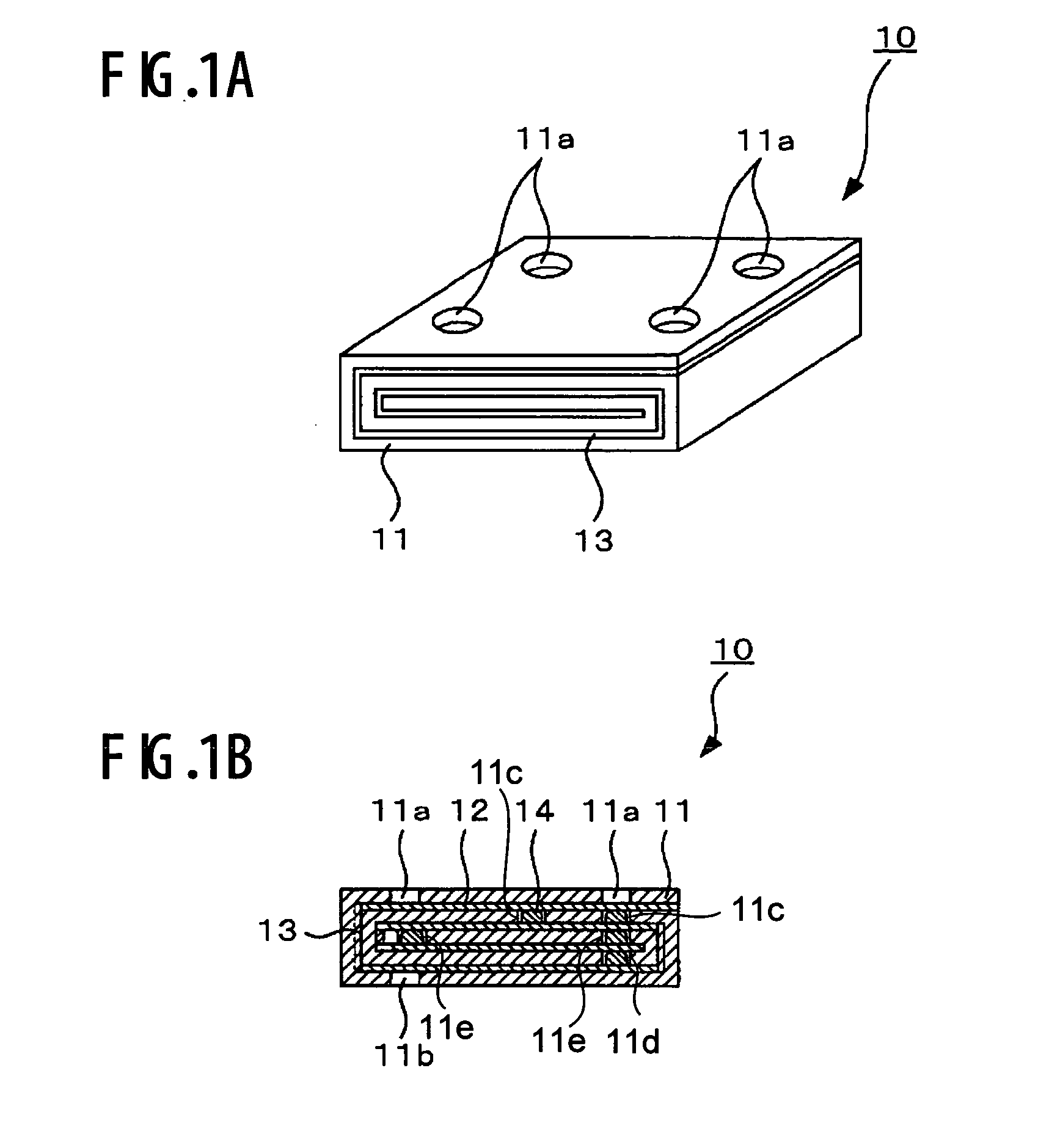
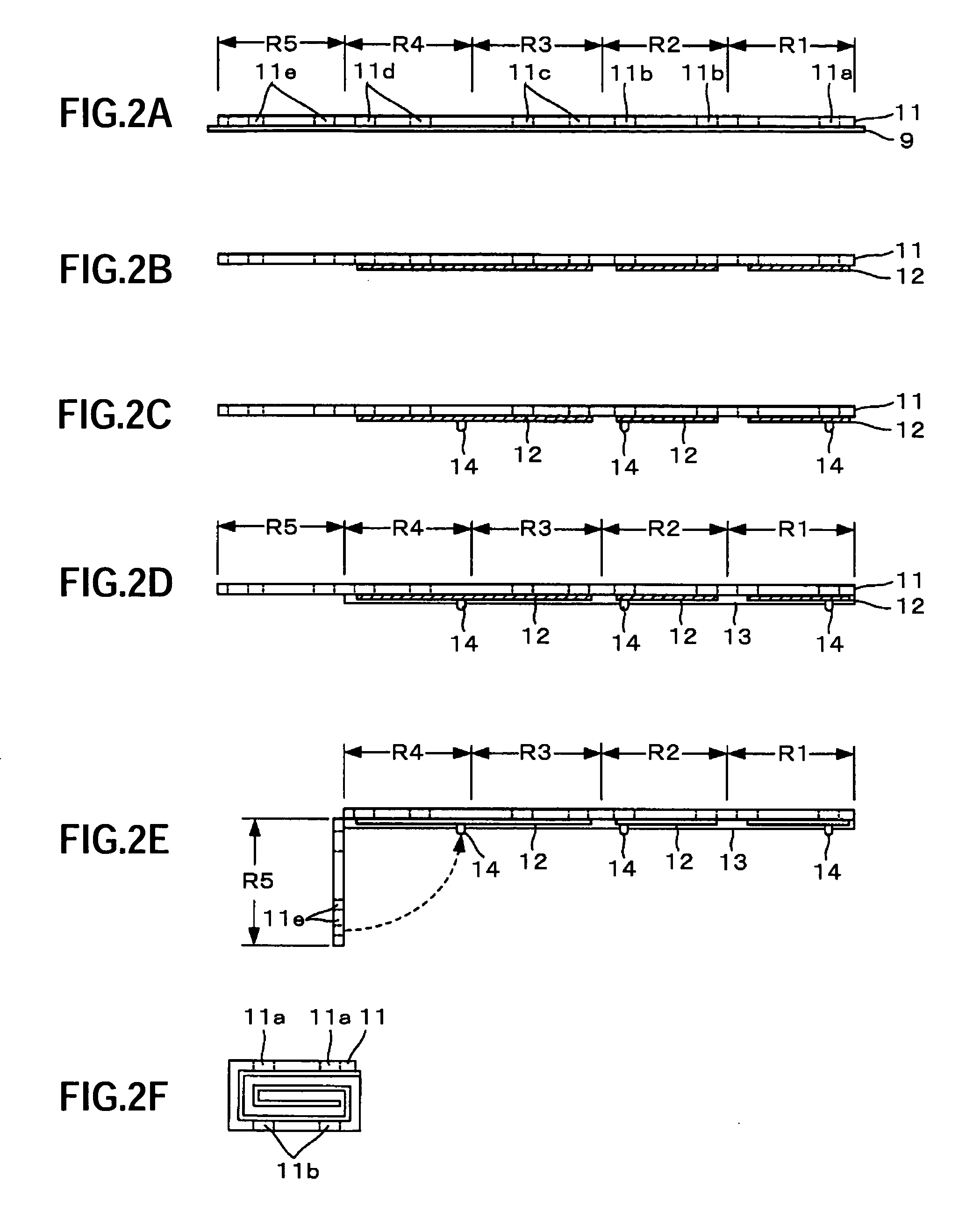
[0043] Hereinbelow, an example of the best mode for carrying out the multilayer wiring board and the process for fabricating a multilayer wiring board of the present invention will be described with reference to FIGS. 1A to 4C.

[0044]FIGS. 1A and 1B show a multilayer wiring board in the present example, wherein FIG. 1A is a perspective view, and FIG. 1B is a transverse sectional view. FIGS. 2A to 2F are cross-sectional views for explaining the fabrication procedure for the multilayer wiring board in the present example, wherein FIG. 2A shows the state in which contact holes are formed in the photosensitive polyimide on a copper foil, FIG. 2B shows the state in which wiring patterns are formed, FIG. 2C shows the state in which bumps are formed, FIG. 2D shows the state in which an insulating bonding layer is formed, FIG. 2E shows the state in which the end portion is bent, and FIG. 2F shows the multilayer wiring board which is folded into a wound structure and cured. FIGS. 3A to 3F ar...


PUM

PropertyMeasurementUnit
thicknessaaaaaaaaaa
lengthaaaaaaaaaa
widthaaaaaaaaaa

Abstract

A multilayer wiring board having a plurality of wiring layers is proposed, which is prepared by a process having the steps of: forming, on one insulating sheet, wiring patterns for all the wiring layers, which patterns are arranged at predetermined positions; and folding the insulating sheet having formed the wiring patterns in the predetermined order and stacking the folded sheet while positioning, and then heating the resultant sheet in a vacuum under a pressure to form a three-dimensional electric wiring.

Description

BACKGROUND OF THE INVENTION [0001] 1. Field of the Invention [0002] The present invention relates to a multilayer wiring board which is suitable for the production of products of a number of types in respectively small amounts in a short term by the so-called build-to-order production in which the production is started after receiving an order, and a process for fabricating a multilayer wiring board. [0003] 2. Description of Related Art [0004] An example of a fabrication process for a conventional, general multilayer printed wiring board is described with reference to FIG. 9. [0005] A multilayer printed wiring board is fabricated as follows. Using a double-sided copper-clad laminate comprising a resin base material which is comprised of an epoxy resin containing, e.g., about 500-mm square glass cloth, and which has both surfaces laminated with a copper foil (S1), a pattern for inner layer of the wiring board is first formed by a so-called photolithography method (S1 to S7). The copp...

Claims


Application Information

Patent Timeline
Patent Type & Authority Applications(United States)
IPC IPC(8): H01B13/00H05K1/00
CPCH05K1/0218H05K1/0393H05K1/16H05K3/4611H05K3/4614Y10T29/49155H05K2201/055H05K2201/0715Y10T29/49135Y10T29/49165H05K3/4635H05K3/46
Inventor WATANABE, YOSHIO
Owner SONY CORP
Why Eureka
Try Eureka