Lead frame and method of manufacturing the same

Active Publication Date: 2006-03-09
HAESUNG CO LTD
View PDF7 Cites 26 Cited by
  • Summary
  • Abstract
  • Description
  • Claims
  • Application Information

AI Technical Summary

Benefits of technology

[0008] The present invention provides a lead frame having an improved wire-bonding of inner leads and an improved soldering of outer leads, and a method of manufacturing the lead frame. The present invention also provides a lead frame having an improved yi

Problems solved by technology

However, this process should be performed through a wet process after the resin molding process, which is often a troublesome process and may result in reduction of the product qualities and reliabilities.
However, the cost of manufacturing the lead frame becomes relatively high because noble metals are used in the process, and cracks may be easily generated during a subsequent bending of the leads (to form a desired shape requiring in the manufacturing process) due to a so-called Galvanic corrosion effect particularly in

Method used


Image

  • Lead frame and method of manufacturing the same
  • Lead frame and method of manufacturing the same
  • Lead frame and method of manufacturing the same

Examples


Embodiment Construction

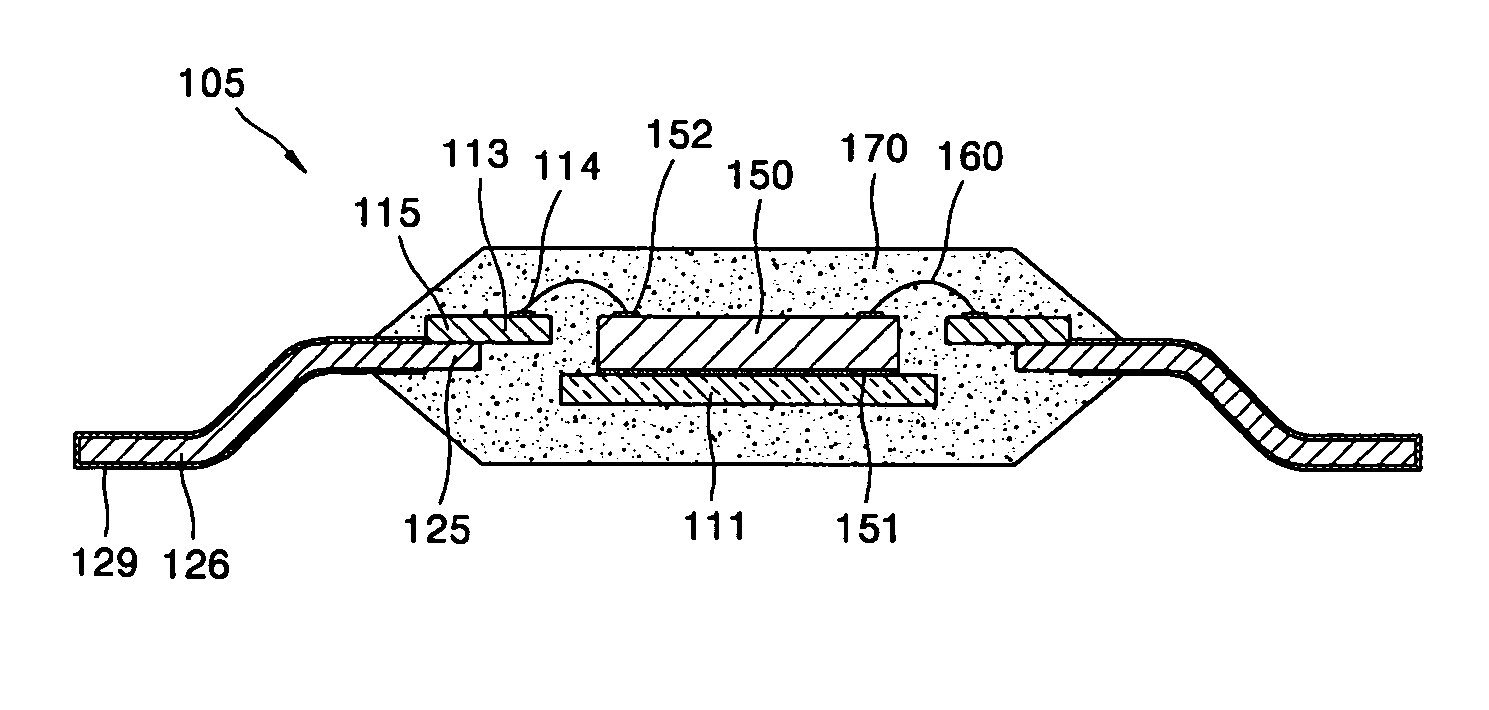
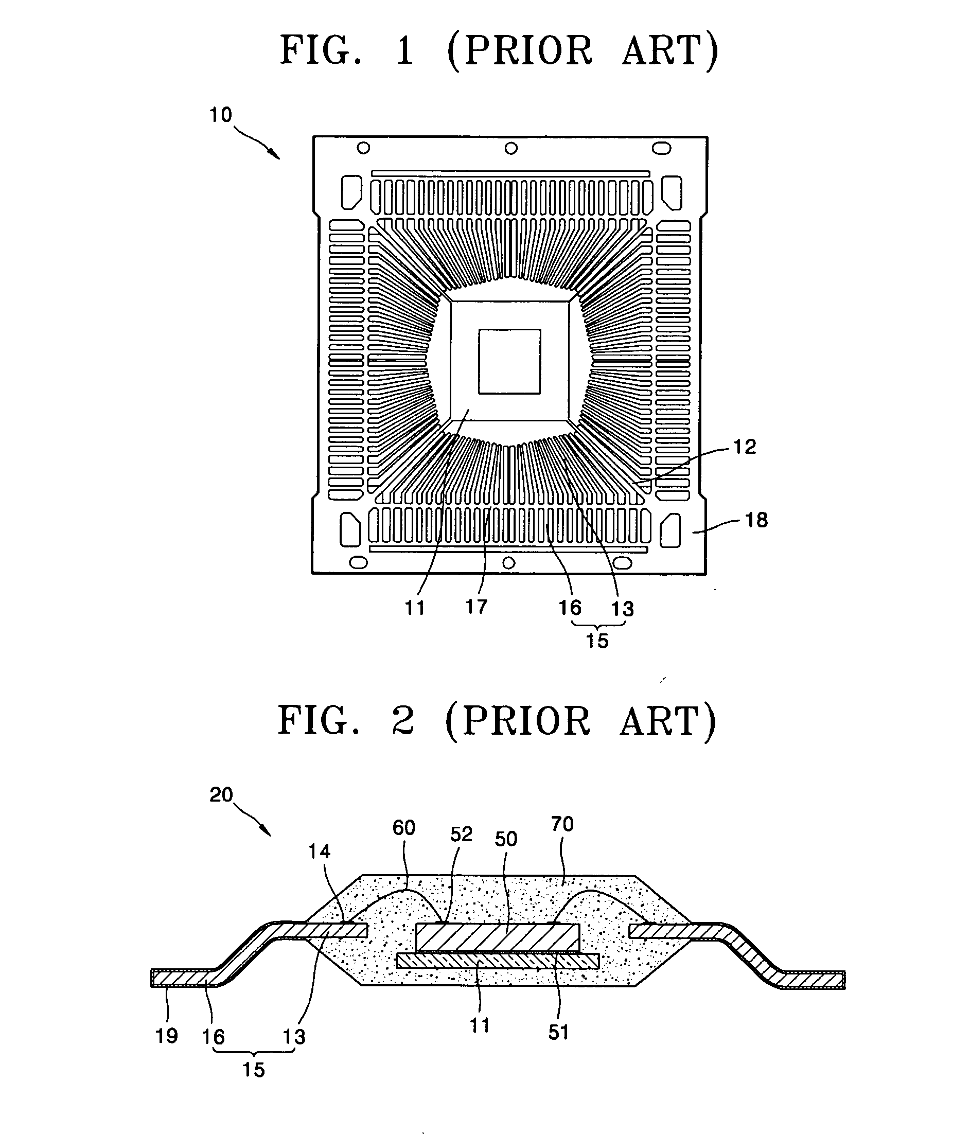
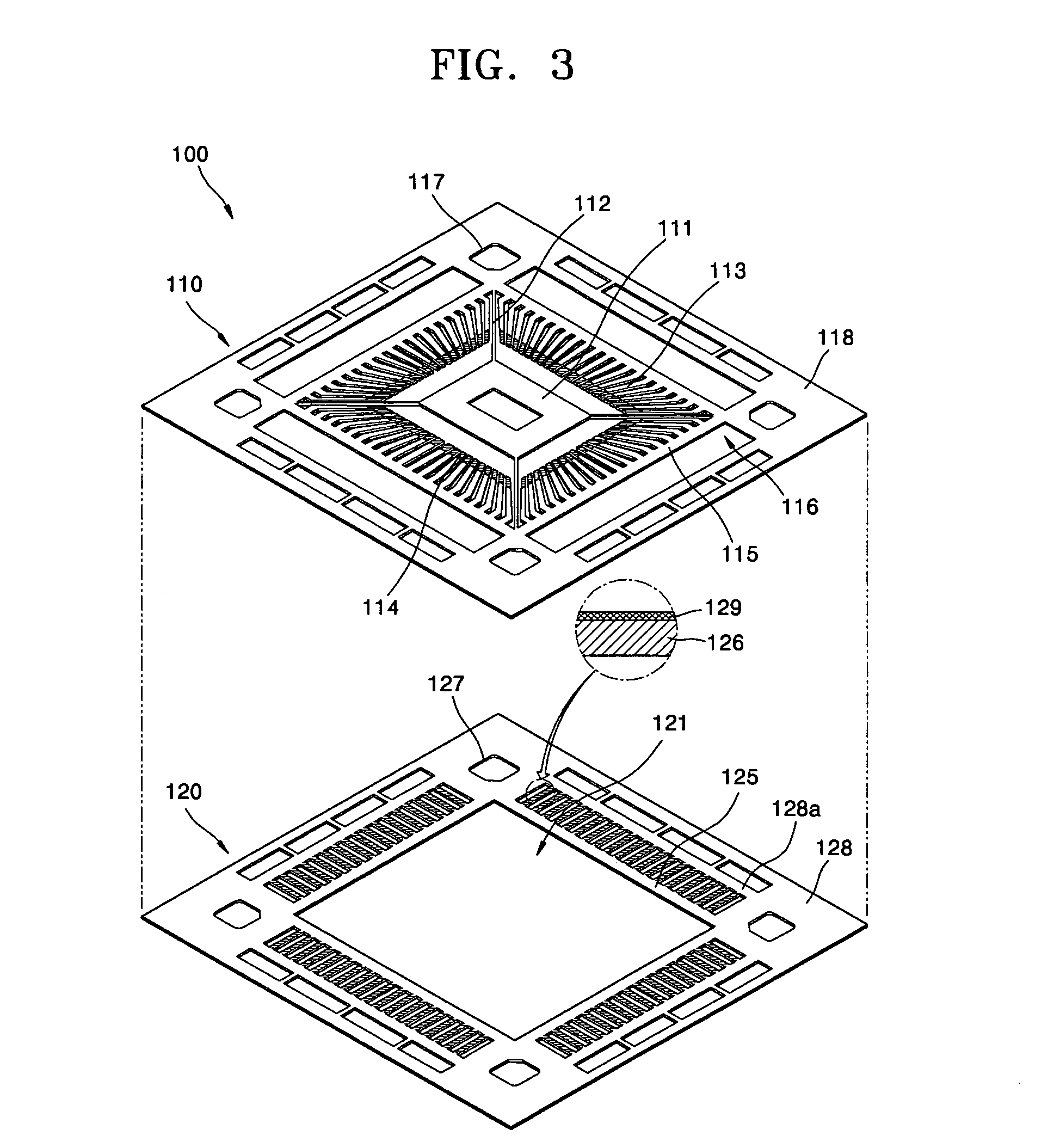
[0029]FIG. 3 is an exploded perspective view of a lead frame constructed according to the present invention, and FIG. 4 is a cross-sectional view of a semiconductor package including the lead frame of FIG. 3. The lead frame shown in FIG. 3 is in a state before performing a coupling portion trimming process that will be described later, and the lead frame in the final form has a different shape with the two lead frames of FIG. 3 coupled with each other and some of the outer portions removed by the trimming process.

[0030] Referring to FIG. 3, a lead frame 100 includes a first lead frame 110 and a second lead frame 120 that are to be coupled or joined to each other in a face-to-face relation by a subsequent process as will be described later. The first lead frame 110 includes a first side rail (i.e., outer frame) 118 forming an outer boundary of the frame, a plurality of inner leads 113 extending generally inwardly (or radially) from the first side rail 118 at predetermined intervals,...


PUM


Abstract

Provided is a lead frame having an improved wire bonding property of inner leads and an improved soldering property of outer leads and preventing defects with high producing yield, and a method of manufacturing the lead frame. The lead frame includes a plurality of inner leads formed with predetermined intervals between them; and a plurality of outer leads extended from the inner leads in length directions of the inner leads, each of which has an end portion overlapped with the inner lead and coupled thereto and the other end connected to neighboring outer lead by a supporting portion.

Description

[0001] This application claims priority of Korean Patent Application No. 10-2004-0070614, filed on Sep. 4, 2004, in the Korean Intellectual Property Office, the disclosure of which is incorporated herein in its entirety by reference. FIELD OF THE INVENTION [0002] The present invention relates to a semiconductor device and a lead frame for the semiconductor device, and a method of manufacturing the lead frame and the semiconductor device. DESCRIPTION OF THE RELATED ART [0003] A lead frame is an element of a semiconductor device, which supports a semiconductor chip thereon and electrically connects the semiconductor chip to an external circuit such as a circuit board. FIG. 1 shows a lead frame 10 according to a conventional art. The lead frame 10 includes a die pad 11 and leads 15 arranged about the die pad 11. The die pad 11 is typically disposed at a central location of the lead frame 10 and connected to an outer frame or side rail member 18 by tie bars 12. The leads 15 include inne...

Claims


Application Information

Patent Timeline
IPC IPC(8): H01L23/495
CPCH01L23/4951H01L2224/0401H01L23/49537H01L23/49582H01L24/48H01L24/85H01L2224/05599H01L2224/05639H01L2224/05644H01L2224/05664H01L2224/16H01L2224/32245H01L2224/48091H01L2224/48247H01L2224/484H01L2224/73215H01L2224/73265H01L2224/85439H01L2224/85444H01L2224/85464H01L2924/01004H01L2924/01028H01L2924/01046H01L2924/01047H01L2924/0105H01L2924/01075H01L2924/01078H01L2924/01079H01L2924/01082H01L2924/014H01L23/49524H01L2924/01033H01L2924/01006H01L2924/00014H01L2224/78H01L2224/45099H01L2924/181H01L2224/4826H01L2924/00012H01L23/495
Inventor LEE, SOO-BONGKIM, JUNG-DOCHOI, WOO-SUKKIM, EUN-HEE
Owner HAESUNG CO LTD
Why Eureka
Try Eureka