

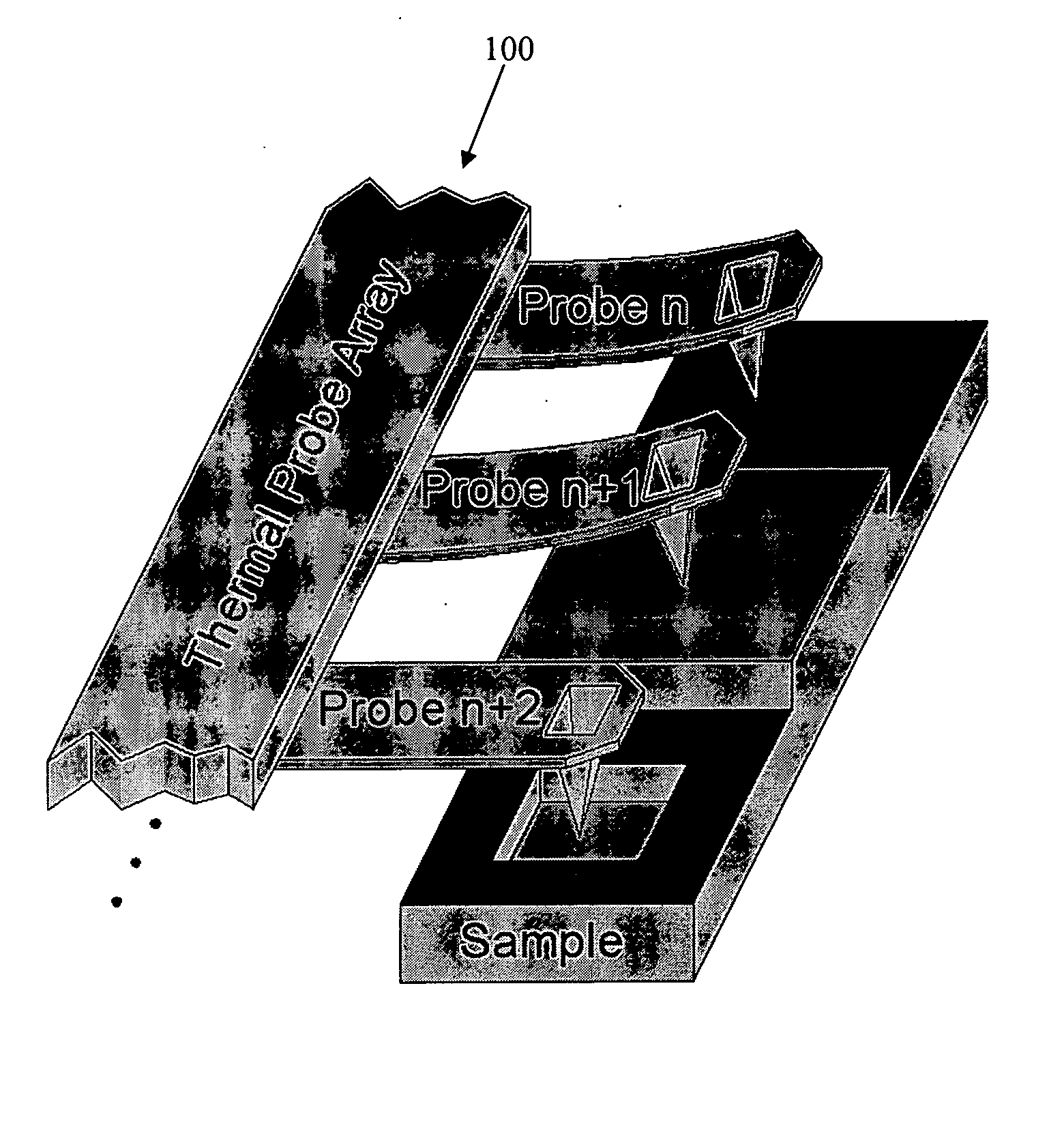
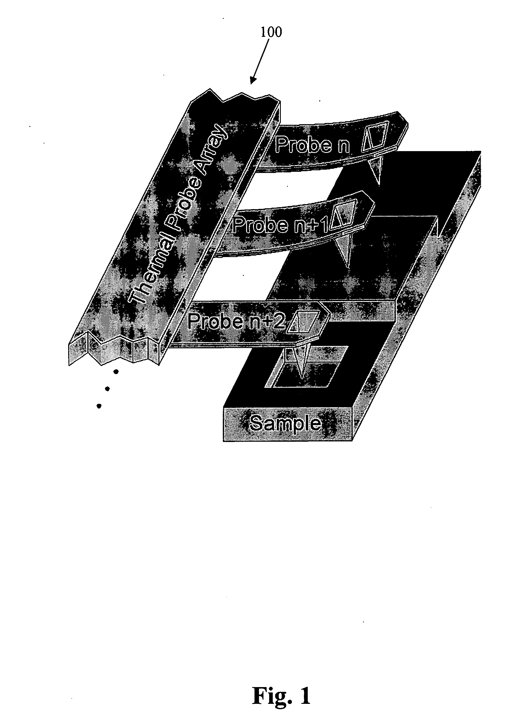
Systems and methods for thin film thermal diagnostics with scanning thermal microstructures
a technology of scanning thermal microstructure and thermal diagnostics, which is applied in the testing/measurement of individual semiconductor devices, semiconductor/solid-state devices, instruments, etc., can solve the problems of different heat flow rate and defects that affect the transient heat flow from the probe to the integrated circuit, and achieve the effect of minimizing the self-heating of the thermal prob
- Summary
- Abstract
- Description
- Claims
- Application Information
AI Technical Summary
Benefits of technology
Problems solved by technology
Method used
Image

Examples
Embodiment Construction
A. Introduction
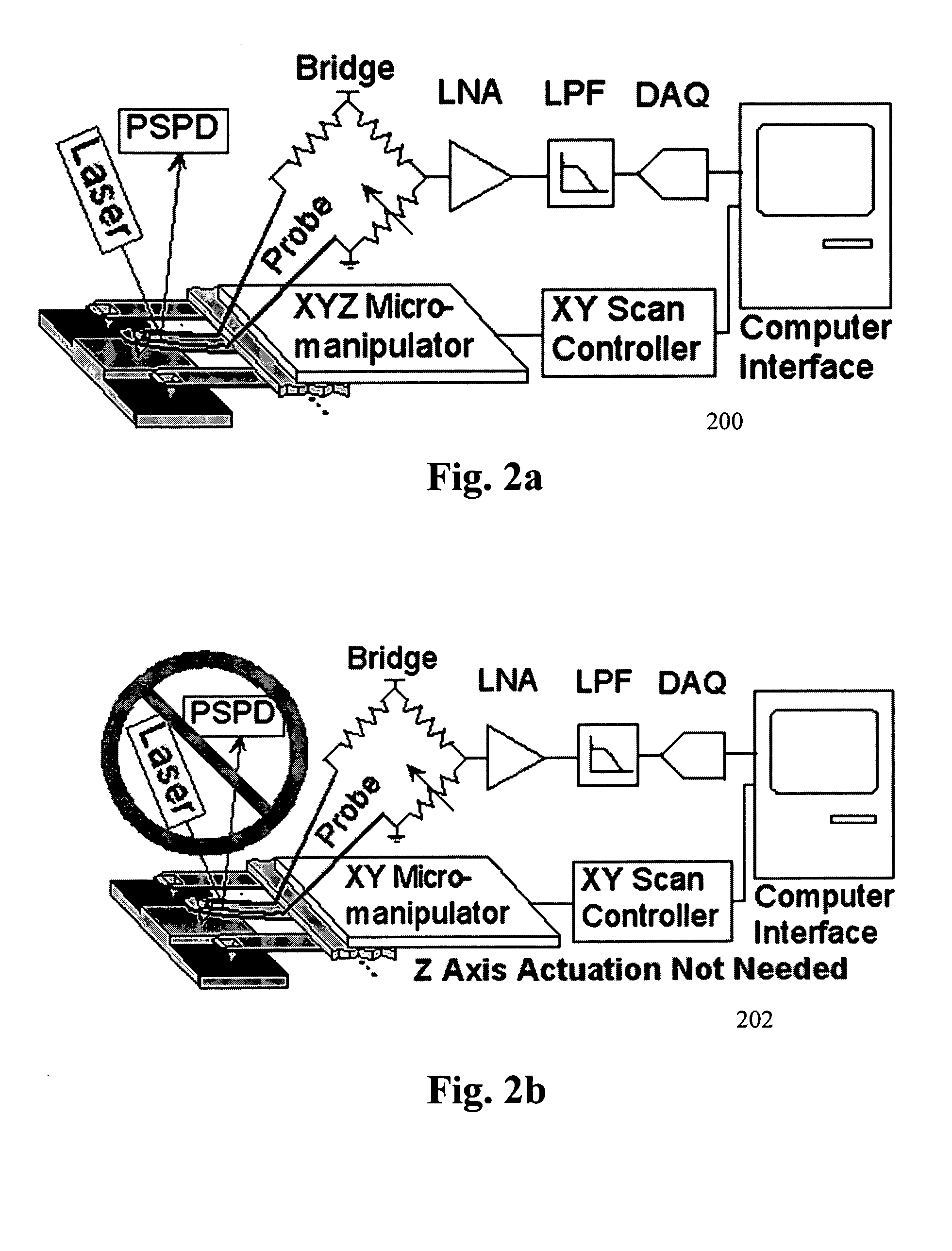
[0024] The invention pertains to the application of a stimulus to a scanning thermal probe and the detection of the thermal interaction between the probe and a sample. Embodiments of the invention may involve the use of one or more of the following techniques: [0025] (a) Observation of the frequency response of probes in proximity to the sample. The relevant observables may include one or more of the following: the difference in phase between the applied stimulus and response, the frequencies of the maxima and minima of the phase difference, the amplitude degradation with frequency, and / or the step response. [0026] (b) Observation of the DC response of probes in proximity of the sample. [0027] (c) Application of a periodic sampling algorithm, whereby a stimulus is applied to a thermal probe for a duration of time smaller than the thermal time constant of the probe, thereby minimizing heating of the thermal probe. In embodiments of the invention, this sampling algorith...
PUM
| Property | Measurement | Unit |
|---|---|---|
| frequency | aaaaa | aaaaa |
| travel distance | aaaaa | aaaaa |
| travel distance | aaaaa | aaaaa |
Abstract
Description
Claims
Application Information