Methods of forming a layer comprising epitaxial silicon, and methods of forming field effect transistors

a technology of epitaxial silicon and forming layers, which is applied in the direction of basic electric elements, electrical apparatus, semiconductor devices, etc., can solve the problems of reducing the breakdown voltage, and reducing the crystal structure of the epitaxial layer

Active Publication Date: 2006-03-09
MICRON TECH INC
View PDF65 Cites 14 Cited by
  • Summary
  • Abstract
  • Description
  • Claims
  • Application Information

AI Technical Summary

Problems solved by technology

Such are non-uniformities in the crystal structure of the epitaxial layer.
Many of these defects are caused by defects appearing at the surface of the substrate which propagate into the layer during growth.
Such can lead to unnecessary recombination generation currents, lower breakdown voltages, higher current leakage and larger junction ideality factors.
Unfortunately, the use of lower temperatures reduces surface mobility and can also result in increased defects over that of higher temperature processing.
This can result in crystallographic defects being generated after growth.
Further, where the epitaxial silicon-comprising material includes germanium, such has an increased tendency for defect formation on the surface during deposition due to mismatched lattice constants of silicon and germanium.
Regardless, after deposition, crystallographic defects are extremely difficult to remove or heal within the bulk epitaxially grown material or at interfaces of such material with other materials.

Method used


Image

  • Methods of forming a layer comprising epitaxial silicon, and methods of forming field effect transistors
  • Methods of forming a layer comprising epitaxial silicon, and methods of forming field effect transistors
  • Methods of forming a layer comprising epitaxial silicon, and methods of forming field effect transistors

Examples


exemplary first embodiment

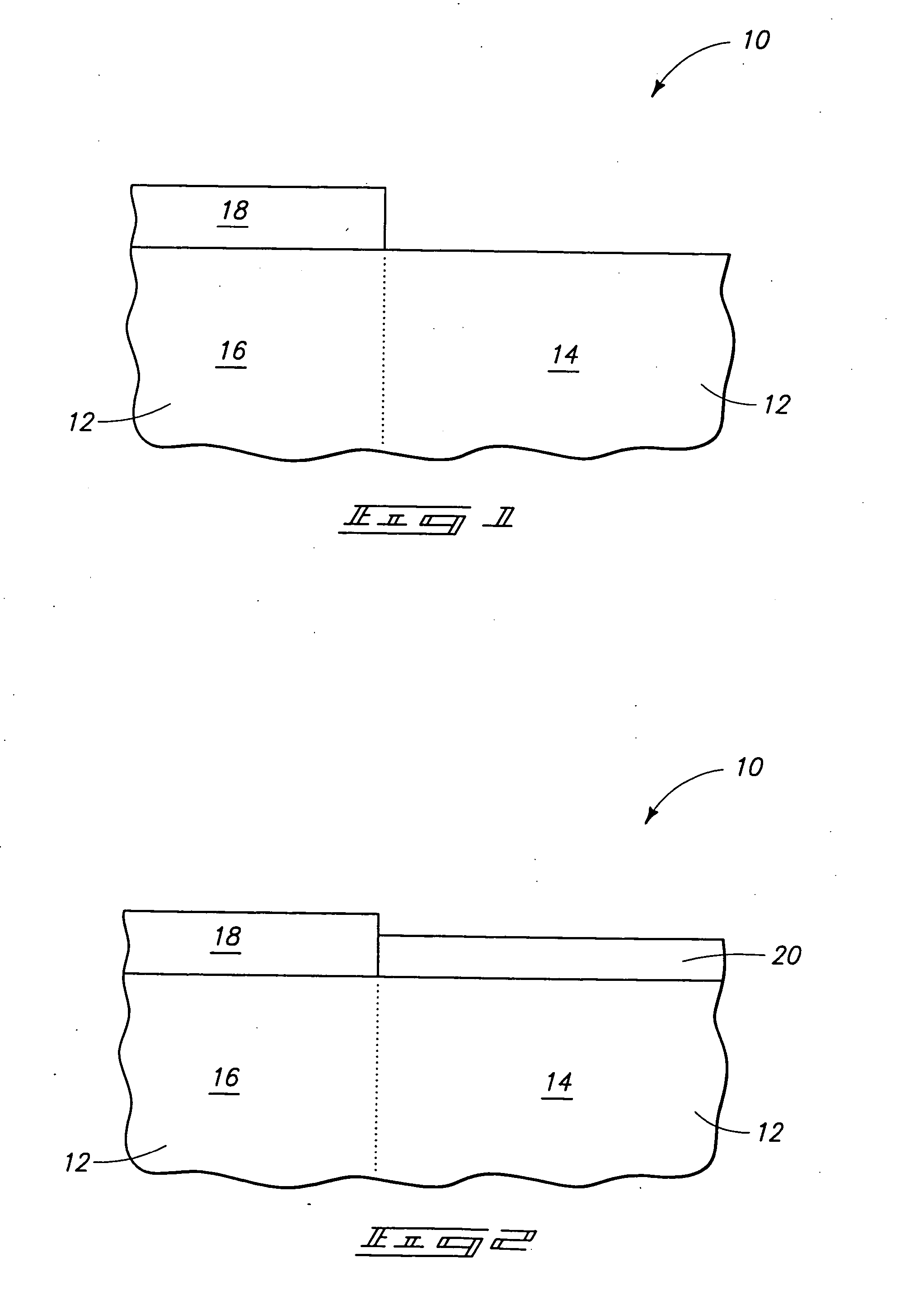
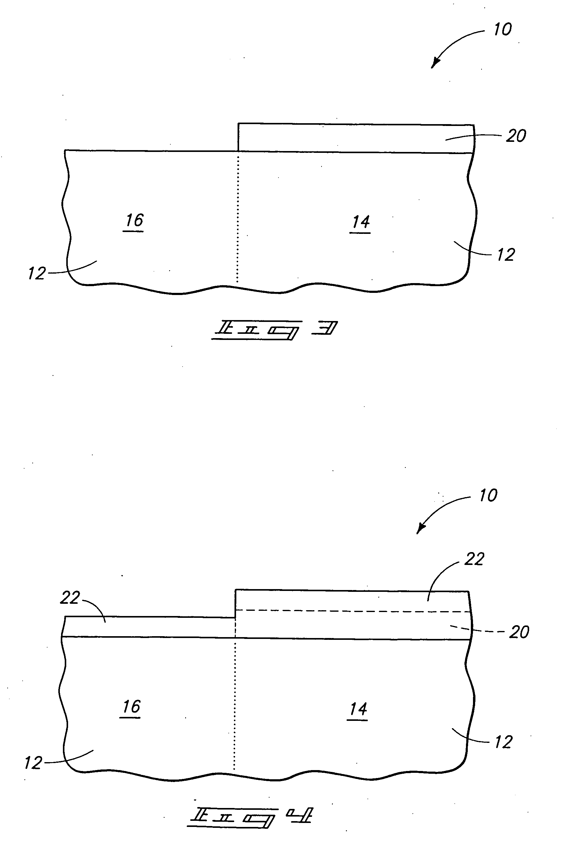
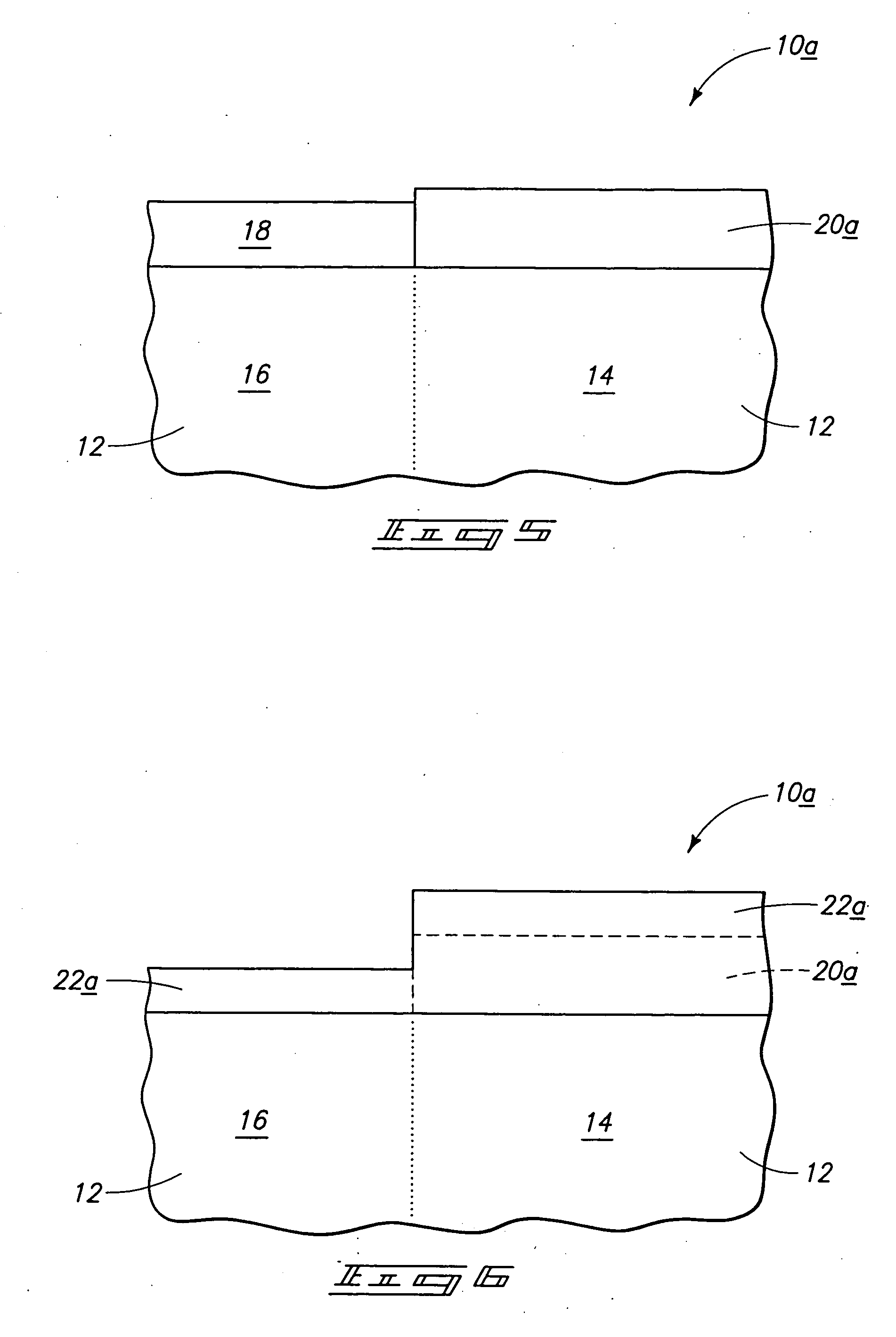
[0040] Exemplary first embodiment methods of forming layers comprising epitaxial silicon are initially described with reference to FIGS. 1-11. Referring to FIG. 1, a substrate, preferably a semiconductor substrate, is indicated generally with reference numeral 10. In the context of this document, the term “semiconductor substrate” or “semiconductive substrate” is defined to mean any construction comprising semiconductive material, including, but not limited to, bulk semiconductive materials such as a semiconductive wafer (either alone or in assemblies comprising other materials thereon), and semiconductive material layers (either alone or in assemblies comprising other materials). The term “substrate” refers to any supporting structure, including, but not limited to, the semiconductive substrates described above. Substrate 10 comprises a monocrystalline material 12, for example and by way of example only, lightly doped monocrystalline silicon or a monocrystalline silicon germanium a...


PUM

PropertyMeasurementUnit
temperatureaaaaaaaaaa

Abstract

The invention includes methods of forming layers comprising epitaxial silicon. In one implementation, an opening is formed within a first material received over a monocrystalline material. Opposing sidewalls of the opening are lined with a second material, with monocrystalline material being exposed at a base of the second material-lined opening. A silicon-comprising layer is epitaxially grown from the exposed monocrystalline material within the second material-lined opening. At least a portion of the second material lining is in situ removed. Other aspects and implementations are contemplated.

Description

TECHNICAL FIELD [0001] This invention relates to methods of forming layers comprising epitaxial silicon. BACKGROUND OF THE INVENTION [0002] Silicon is a common semiconductive material used in the fabrication of integrated circuits. Silicon can occur in crystalline and amorphous forms, and when crystalline can be monocrystalline or polycrystalline. In some instances, silicon is combined with germanium, essentially forming a silicon germanium alloy. Such materials can be doped with conductivity enhancing impurities (i.e., boron and / or phosphorus) to modify the conducting characteristics of the silicon-comprising material. [0003] Monocrystalline silicon can be provided in bulk substrate form or otherwise grown or deposited epitaxially from an exposed monocrystalline material. Epitaxy generally involves the growth or deposition of a single or monocrystalline layer of material such that the epitaxial layer has a crystal orientation which is common to that of the material from which it is...

Claims


Application Information

Patent Timeline
Patent Type & Authority Applications(United States)
IPC IPC(8): H01L21/20
CPCH01L29/66787H01L21/02642H01L21/0262H01L21/0245H01L21/02532H01L21/02381
Inventor BLOMILEY, ERIC R.SANDHU, GURTEJ S.BASCERI, CEMRAMASWAMY, NIRMAL
Owner MICRON TECH INC
Why Eureka
Try Eureka