Bump structure of semiconductor package and method for fabricating the same

a semiconductor package and bump technology, applied in the direction of semiconductor/solid-state device details, printed circuit aspects, printed circuit manufacturing, etc., can solve the problems of bridging or short circuit of bumps, adversely affecting the reliability of semiconductor packages, and the functional complexity of semiconductor elements has become more complicated, so as to reduce the formation of voids and increase spacing

Inactive Publication Date: 2006-03-09
SILICONWARE PRECISION IND CO LTD
View PDF1 Cites 80 Cited by
  • Summary
  • Abstract
  • Description
  • Claims
  • Application Information

AI Technical Summary

Benefits of technology

[0009] In light of the drawbacks in the prior art, a primary objective of the present invention is to provide a bump structure of a semiconductor package and a method for fabricating the same, so as to increase spacing between adjacent bumps and reduce formation of voids.

Problems solved by technology

However, since the functionality of the semiconductor element has become more complicated, the bumps are accordingly arranged in higher density.
This adversely affects the reliability of the semiconductor package, and even leads to bridging or short circuit of the bumps 101 after the reflow process.
Particularly when the number of I / O connections of the semiconductor element is increased and the pitch between adjacent pillar bumps is reduced to below about 150 μm, the similar drawback is produced that the underfill material fails to penetrate and fill small spaces between the adjacent pillar bumps, thereby causing the problem of voids or short circuit, etc.

Method used


Image

  • Bump structure of semiconductor package and method for fabricating the same
  • Bump structure of semiconductor package and method for fabricating the same
  • Bump structure of semiconductor package and method for fabricating the same

Examples


Embodiment Construction

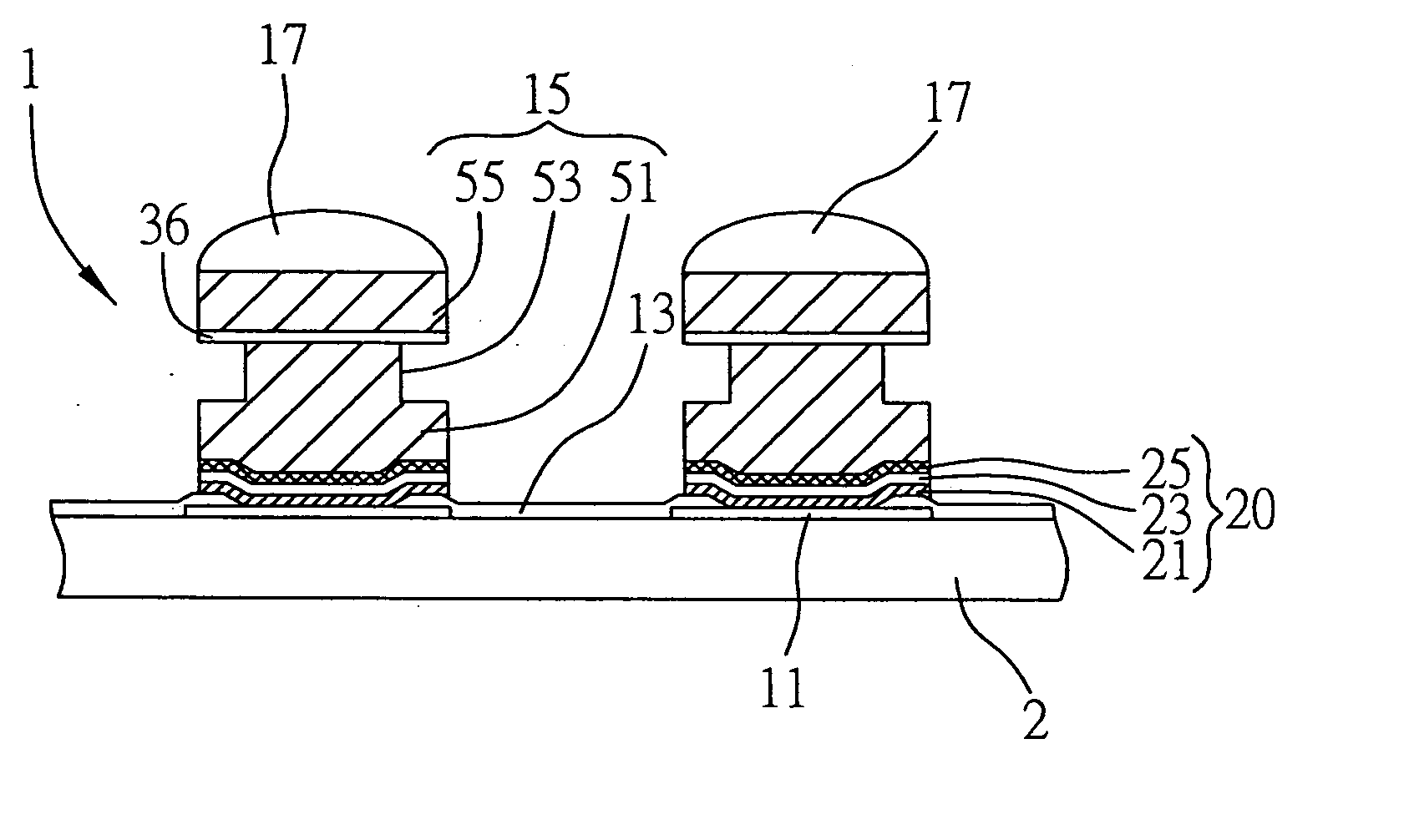
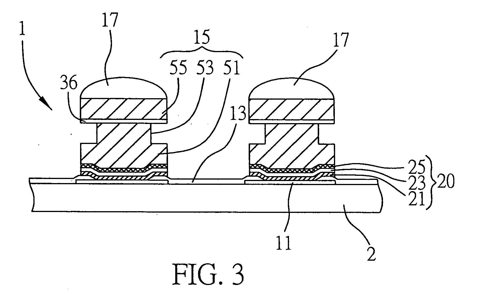
[0025] FIGS. 3 to 5B are schematic diagrams showing a bump structure of a semiconductor package and a method for fabricating the bump structure according to preferred embodiments of the present invention. It should be noted that the drawings are simplified schematic diagrams and only show the basic structure and relevant components according to the present invention. The number, shape and size of the components are not drawn in real scale, and the arrangement of components should be much more complex in practice.

[0026]FIG. 3 shows the bump structure 1 of a semiconductor package in this embodiment. The bump structure 1 is used for connecting a semiconductor element 2 to a carrier. The semiconductor element 2 has a plurality of electrical connection pads 11 and a passivation layer 13 thereon, with the electrical connection pads 11 being exposed from the passivation layer 13. The bump structure 1 comprises an under bump metallurgy (UBM) layer 20, an I-shaped conductive pillar 15, and ...


PUM


Abstract

A bump structure of a semiconductor package and a method for fabricating the same are provided. The bump structure is used to connect a semiconductor element to a carrier of the semiconductor package. The fabrication method primarily employs an electroplating process to form the bump structure including an under bump metallurgy (UBM) layer, at least one I-shaped conductive pillar, and a solder material. This allows fine-pitch electrical connection pads to be arranged in the semiconductor package, and also provides an enhanced support structure and a sufficient height between the semiconductor element and the carrier.

Description

FIELD OF THE INVENTION [0001] The present invention relates to bump structures of semiconductor packages and fabrication methods thereof, and more particularly, to a bump structure of a flip-chip semiconductor package, and a method for fabricating the bump structure. BACKGROUND OF THE INVENTION [0002] Along with the development of light-weight and small-profile electronic products, semiconductor packages serving as core components of the electronic products have accordingly been miniaturized in size. Preferably, the semiconductor packages with a reduced size, fine-pitch interconnections and high-density I / O (input / output) connections, such as a flip-chip package, ball grid array (BGA) package, and chip size package (CSP), etc., have become mainstream package products in the market. [0003] For example, in a conventional flip-chip semiconductor package 10 shown in FIG. 1, a plurality of bumps 101 are formed on an active surface of a semiconductor element 103 such as a semiconductor ch...

Claims


Application Information

Patent Timeline
Patent Type & Authority Applications(United States)
IPC IPC(8): H01L21/44
CPCH01L21/4853H01L2224/73204H01L24/11H01L24/12H01L2224/13023H01L2224/1308H01L2224/13084H01L2224/13111H01L2224/13116H01L2224/13118H01L2224/13139H01L2224/13144H01L2224/13147H01L2224/13155H01L2224/13164H01L2224/16225H01L2924/01013H01L2924/01022H01L2924/01029H01L2924/0103H01L2924/01046H01L2924/01047H01L2924/01078H01L2924/01079H01L2924/01082H05K3/4007H05K2201/0367H05K2201/09845H05K2203/0723H01L23/49816H01L2224/32225H01L2224/11902H01L2924/014H01L2924/01033H01L2924/01023H01L2924/00013H01L2924/00014H01L2224/13099H01L2924/00H01L24/03H01L24/05H01L24/13H01L2224/05001H01L2224/05022H01L2224/05023H01L2224/05027H01L2224/0508H01L2224/05124H01L2224/05147H01L2224/05155H01L2224/05166H01L2224/05568H01L2224/05611H01L2224/05644H01L2224/05647H01L2224/13017H01L2224/13018H01L2924/013
Inventor LIN, YING-RENHUANG, CHIEN-PINGTSAI, HO-YIHSIAO, CHENG-HSU
Owner SILICONWARE PRECISION IND CO LTD
Why Eureka
Try Eureka