
Structure and method for enhanced uni-directional diffusion of cobalt silicide

Inactive Publication Date: 2006-03-16
GLOBALFOUNDRIES INC
View PDF6 Cites 24 Cited by
  • Summary
  • Abstract
  • Description
  • Claims
  • Application Information

AI Technical Summary

Benefits of technology

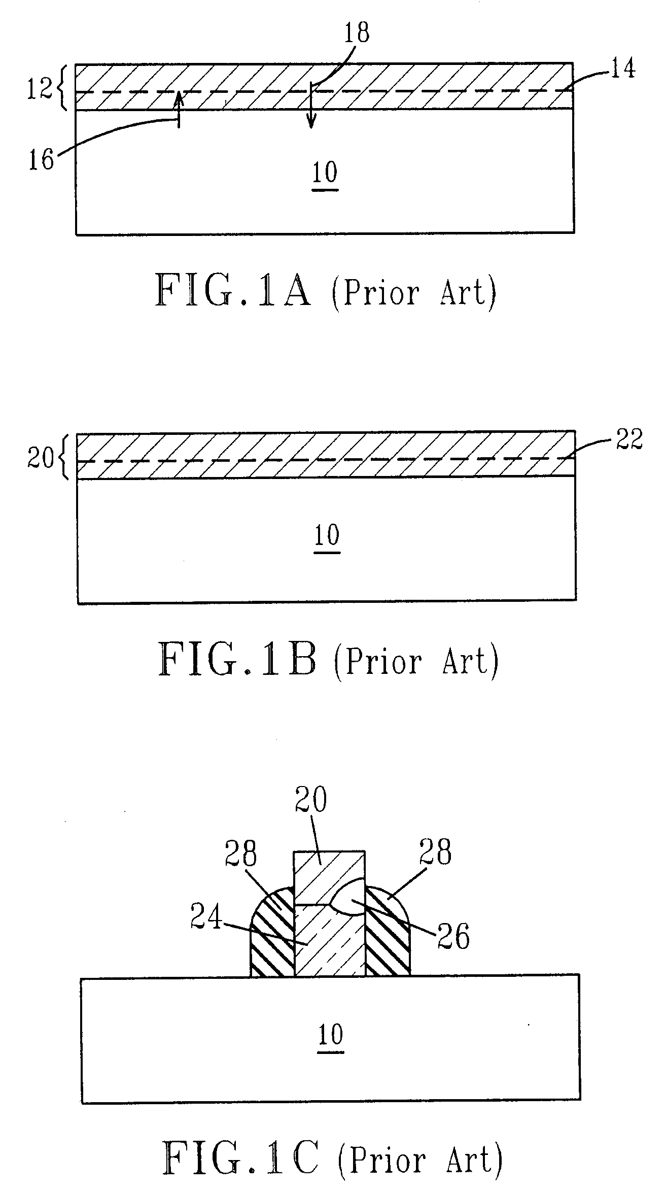
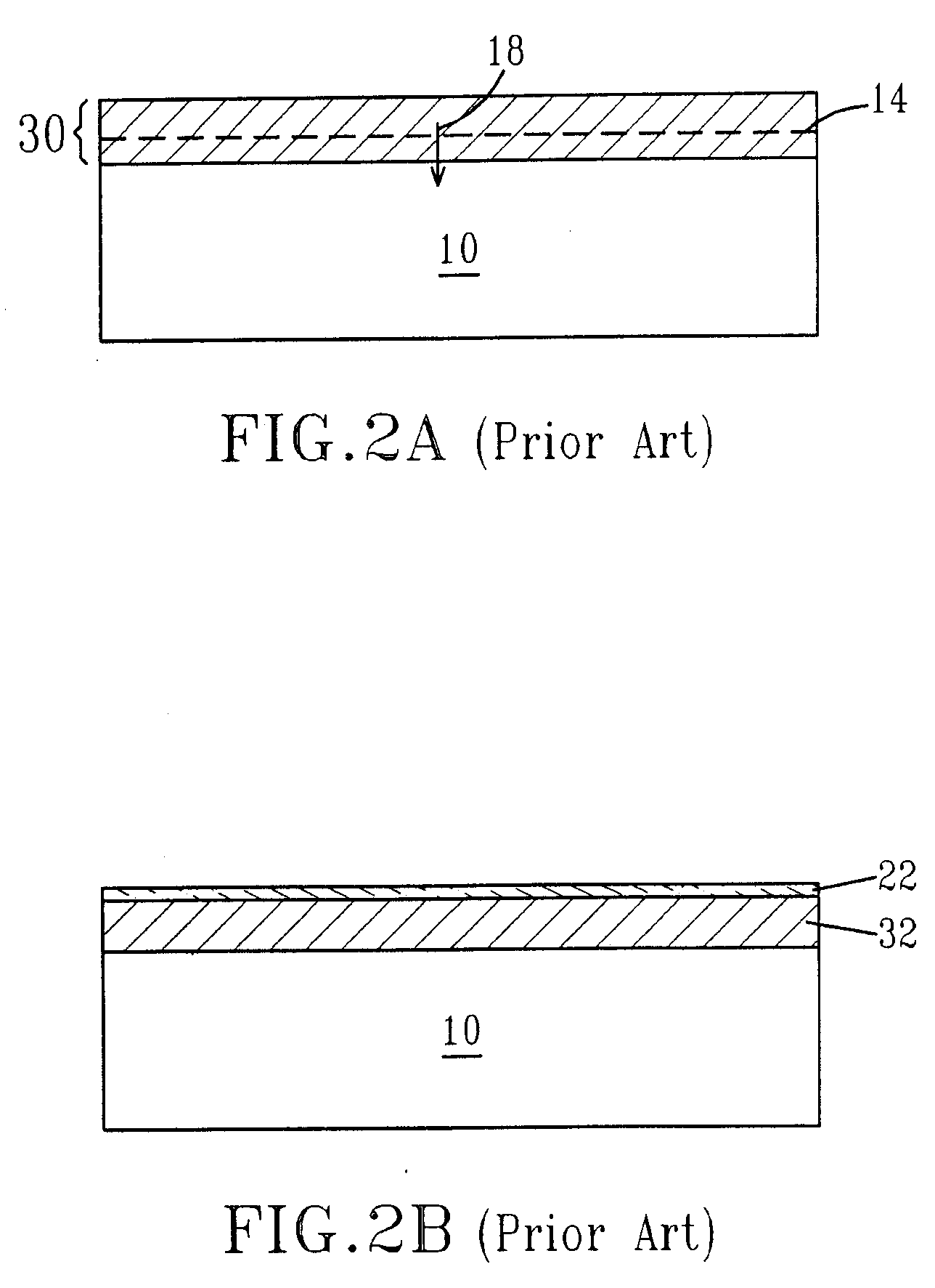
[0015] The present invention provides a method that further improves the suicide process disclosed in Brodsky, et al. Thus, the advantages mentioned in the Brodsky, et al. process, i.e., reducing Si consumption and bridging during suicide formation, are also achieved in the present invention. The improvement of the method of the present invention over the process disclosed in Brodsky, et al. is that the resultant metal silicide has an increased self-limiting thickness. That is, the method of the present invention provides a technique for fabricating metal silicide contacts that have an increased self-limiting thickness, thereby forming a metal silicide that will not be totally removed during the formation of metal interconnects to the metal silicide contact.
[0016] As indicated above, the Brodsky, et al. process provides a metal silicide whose thickness is about 12 nm. Such a thin metal silicide will be entirely, or substantially removed during subsequent interconnect processing steps. The entire or substantial removal of the metal silicide causes contact resistant problems with the metal to diffusion contact. This contact resistant problem is avoided in the present invention since the metal silicide formed has a thickness from about 14 to about 25 nm, preferably about 18 to about 25 nm. The increased thickness in the metal silicide contact is important in the semiconductor industry since it allows for the formation of metal contacts to the metal silicide contacts that have a lower portion (including sidewalls and a bottom wall) that is completely embedded within the silicide contact.
[0017] Moreover, the method of the present invention provides a structure including a thick metal silicide where low leakage is exhibited. By “low leakage”, it is meant that there is little or no metal silicide that forms atop the trench isolation regions that are present in the structure.

Problems solved by technology

The entire or substantial removal of the metal silicide causes contact resistant problems with the metal to diffusion contact.

Method used


Image

  • Structure and method for enhanced uni-directional diffusion of cobalt silicide
  • Structure and method for enhanced uni-directional diffusion of cobalt silicide
  • Structure and method for enhanced uni-directional diffusion of cobalt silicide

Examples


Embodiment Construction

[0026] The present invention, which provides a method of forming a metal silicide atop a Si-containing material utilizing a first anneal that includes two distinct thermal cycles as well as the structure that is formed from the inventive method, will now be described in greater detail. It is noted that the drawings of the present application are provided for illustrative purposes and thus they are not drawn to scale.

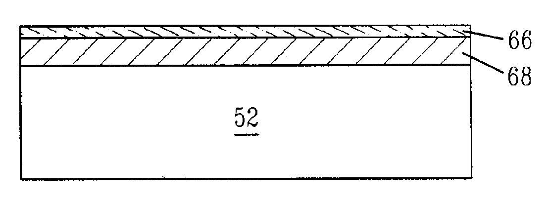
[0027] Reference is made to FIGS. 3A-3F which illustrate the basic processing steps of the present invention that are capable of forming a CMOS structure containing a low resistance thick metal silicide in which the Si consumption and the bridging has been significantly reduced. By “thick”, it is meant a metal silicide that has a thickness from about 14 to about 25 nm. Specifically, FIG. 3A illustrates an initial structure 50 that is formed after the first step of the present invention has been performed. Specifically, the structure 50 comprises a Si-containing material...


PUM


Abstract

The present invention provides a method for enhancing uni-directional diffusion of a metal during silicidation by using a metal-containing silicon alloy in conjunction with a first anneal in which two distinct thermal cycles are performed. The first thermal cycle of the first anneal is performed at a temperature that is capable of enhancing the uni-directional diffusion of metal, e.g., Co and / or Ni, into a Si-containing layer. The first thermal cycle causes an amorphous metal-containing silicide to form. The second thermal cycle is performed at a temperature that converts the amorphous metal-containing silicide into a crystallized metal rich silicide that is substantially non-etchable as compared to the metal-containing silicon alloy layer or a pure metal-containing layer. Following the first anneal, a selective etch is performed to remove any unreacted metal-containing alloy layer from the structure. A second anneal is performed to convert the metal rich silicide phase formed by the two thermal cycles of the first anneal into a metal silicide phase that is in its lowest resistance phase. A metal silicide is provided whose thickness is self-limiting.

Description

BACKGROUND OF INVENTION [0001] The present invention relates to semiconductor devices, and more particularly to a method of enhancing the uni-directional diffusion of a metal during silicidation using an initial anneal that includes two distinct thermal steps (hereinafter thermal cycles). The present invention also relates to semiconductor structures that include the metal silicide produced using the method of the present invention. [0002] One type of material commonly employed in fabricating ohmic contacts for semiconductor devices is metal suicides such as cobalt silicide (CoSi) or nickel silicide (NiSi). Metal suicides are typically fabricated using a conventional self-aligned silicide (i.e., salicide) process. In such a process and when CoSi contacts are desired, a blanket TiN / Co film is deposited over exposed Si-containing regions (e.g., source, drain and gate). A first annealing step that is performed at a temperature from about 400° to about 600° C. is then employed to form a...

Claims


Application Information

Patent Timeline
IPC IPC(8): H01L21/44
CPCH01L29/665H01L21/28518H01L21/24
Inventor DOMENICUCCI, ANTHONY G.JONES, BRADLEY P.LAVOIE, CHRISTIANPURTELL, ROBERT J.WANG, YUN YUWONG, KWONG HON
Owner GLOBALFOUNDRIES INC
Learn More